Need Guidance for cross talk control -2040 RP

Hi,
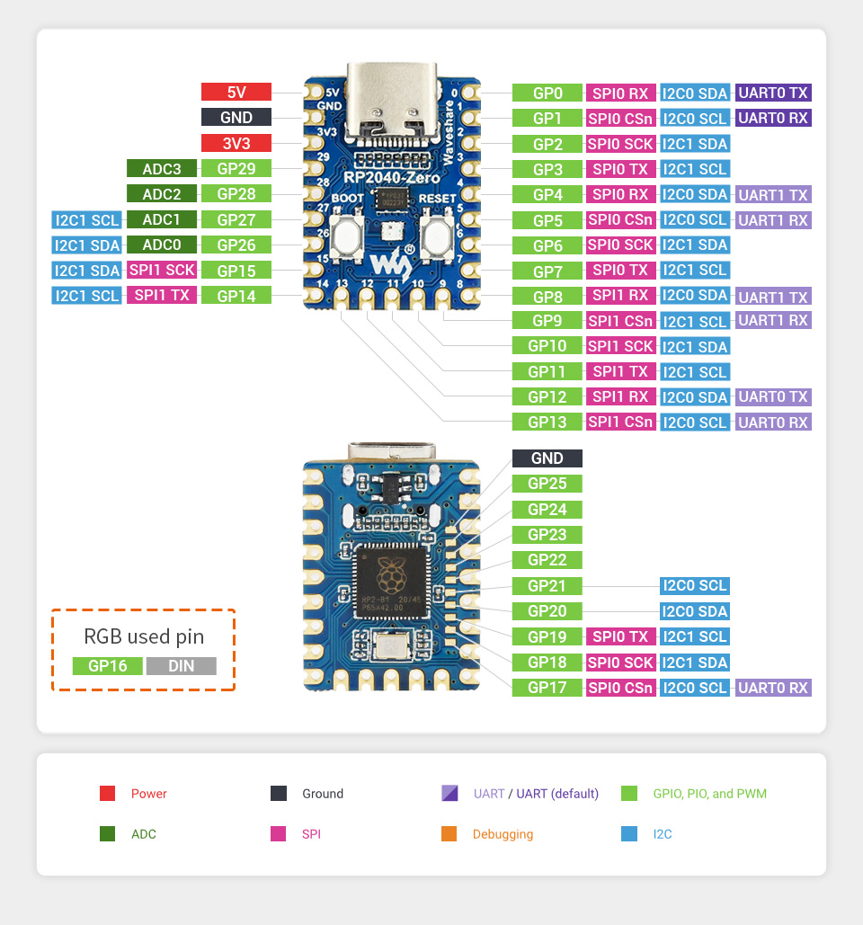
I apologize for the interruption, but I am currently facing an issue with calibrating three RP-2040 microcontrollers (each with 12-bit 4-channel ADCs). I am providing an AC sine wave as the input signal and using G14 as the trigger signal.

The problem arises when I measure the voltage signal of individual ADC channels and compare it to the voltage signal when all channels are connected. Additionally, I have taken background measurements. Could you please guide me on how to control or minimize the crosstalk between neighboring channels?

Kind regards

Hasham

1 Like

Hi Hasham
What do you mean by “crosstalk”
Surely with all channels connected to the one sine wave source the “crosstalk” would be 100%
I think the term “crosstalk” is being misused here.

The way to measure “crosstalk” is to feed the signal into one channel and measure how much of that signal appears on the other 2 channels with no signal input.
Cheers Bob

2 Likes

Hi Bob,
Thank you for your response and guidance; I tried connecting one channel to the input sine wave signal and grounding the other channels. Despite this, I observed some signals in the neighboring channels that were connected to ground.

Is there a way to minimize or control this crosstalk between neighboring channels? I noticed small dips in the averages of individual channels when I graphed them. How can I minimize these dips?

I have also attached an image of an Excel file showing the data for individual channels and their graph behavior for your reference.

Kind regards
Hasham

2 Likes

Are you using GPIO23 to control the operation of the PSU to provide a stable reference voltage? Without this control, random fluctuations in all channels of the ADC are likely (although even with a clean reference they won’t all disappear).

Have you actually referenced the fluctuations in the zero-level readings to the signal input level? You need to do this to demonstrate crosstallk, as distinct from other sources of variation. Have you confirmed that the fluctuations you are seeing are outside the specified error range of the ADC?

5 Likes

Hi Hasham
Just what that means is not clear. Just a bunch of numbers in a spreadsheet is all I can make out. What do they represent.

You have a graph with 2 sine waves shown. At what frequency and what amplitude. There is no indication of what the X and Y axes represent so it means nothing.

Getting on to “cross talk”. Neatness and layout of wiring can have an influence but would be more apparent at higher frequencies.
You say you feed a signal into one channel and ground the others and see evidence of the original signal on the grounded channels. At what relative levels. This might suggest some cross coupling between channels in the ADC itself which you can probably do nothing about. Is there a spec for this in the ADC data sheet. This might be normal and what you are trying to do might be outside the designed usage. Just don’t know with the supplied information.
Cheers Bob

2 Likes

Hi Bob,

Thank you for your response, and I apologize for my delayed reply. You are correct; I need to focus on the neatness and layout of the wires. I will share more detailed graphs, addressing the points you mentioned.

Once again, thank you.
Hasham

2 Likes

Hi Jeff,
Thank you for your response, and I apologize for the delayed reply. Yes, you are correct; I am providing a stable reference voltage as the trigger signal from GP14. However, I have not set the fluctuations to zero level readings, as they range from just 10 mV to 15 mV.

Could you please guide me on how to set these fluctuations to zero to better observe the crosstalk? Additionally, how can I confirm that the fluctuations are outside the specified error range of the ADC?

Kind regards

Hasham

1 Like

Hi Hasham

I don’t know much about RPi but just what do you mean by that.

A schematic of EXACTLY what you have would be helpful.

I just looked at the pin connections of a typical 2040 device and GP14 seems to be a general purpose in/out. NOT really a reference for an ADC. Could be anything across a range of ACTUAL voltages I think as long as it meets some sort of digital criteria.

You have not stated which actual device you have. As I understand it “RP2040” is the Micro processor chip itself and used on different devices from different vendors with probably some difference in utilisation and pin outs. So this little gem of information would be of some help also.
Cheers Bob

PS You don’t seem to have divulged which actual ADC you are using either. No information would get you very little in the way of advice or solutions. Any advice could only be made on guesswork which I for one am very reluctant to do. Very time consuming.

2 Likes

Hi Hasham,

To echo others here it would be brilliant if you could share some images of your setup. This way we know what you are working with. Currently, I can’t see where your other two RP2040 boards come into play. If you could share some more details on what your end goal is with this project that would also be great.

2 Likes

Firstly, don’t assume that crosstalk is the problem. That assumption will prevent you from looking at other places where the measurement variations are coming from and creates the likelihood that you will miss the actual cause. If you are using a Pico then reference stabilisation is done by controlling the PSU mode through GPIO23 as described in the Pico refrence. If you are not using a Pico then you must ensure a stable supply to the ADC VRef using whatever means is relevant for your setup. Whatever you choose, the trigger signal and GPIO14 are not involved.

I assume you mean fluctuations in the ADC VRef, because there is no way to tell you how to get the fluctuations in the measurements to zero until the cause is identified. The steps you would take to remove fluctuations in VRef will depend on how you are powering the chips.

Note that you should also check the revision number of your chips, as earlier models (prior to revision E6) did not disable digital input for the ADC pins, creating some random fluctuations.

The specified ENOB and other error parameters are set out in the RP2040 datasheet.

4 Likes

Hi Jeff,

Thank you for your guidance. I was initially confusing crosstalk with calibration. In my setup, I am using a PICO RP2040 where the trigger signal (reference voltage) is connected to GP14. I’ve programmed the Picomite to set a trigger value for a falling edge, which means the trigger should activate when the signal reaches 0.8 V. However, I’m encountering an issue where the output voltages I’m getting are higher than expected—they should be lower or close to 0.8 V. The trigger signal frequency is set at 360 Hz, and the input voltage is a 1.2 V AC sine wave at the same frequency. Currently, the output voltages from all ADC channels are between 0.85 and 0.87 V. When I increase the frequency to 400 Hz, 450 Hz, or 500 Hz, the output voltages rise even higher, which is confusing. Could you please help me identify where I might be making a mistake?
Kind regards

Hasham


{this is PicoMite code}
other 3 codes for PICOs are same as it is.

OPTION EXPLICIT
OPTION VCC 3.322        'as measured with a DMM
'PICO #1                'set as required

'options to be set using the terminal
'this only needs to be done once
'OPTION POWER PWM
'OPTION CASE UPPER
'OPTION CPUSPEED 378000
'OPTION AUTORUN ON

'This program triggers an ADC conversion when it receives a
'pulse on the trigger input (GP14)
'Version 2a:  try different ways to compress the data. Trying STR2BIN(UINT16....
'             note - the code below suits all the PICOs. Just comment out what's
'             not required. Removed 'pulldown' on the trigger input. Set PICOs
'             cpuspeed to 378MHz for reliable serial transfer
'Version 2:   PICO0 does 2 jobs, it collects data for channels 0-3 and also
'             collects data from the other PICOs and sends it all to the computer
'             Just comment out or enable lines as described for the different PICOs
'Version 1a:  single channel working, now try all 4 channels on a PICO mini
'version 1:   basic operation, single channel, written by Peter Ihnat, 5/2024

'arrays to hold the ADC data
DIM da0(1),da1(1),da2(1),da3(1)
'strings to hold the compressed data
DIM dstring1$,dstring2$

'make each data collecting PICO wait a different delay time before sending data
'so that the data being sent is sequential without any overlap
'simply enable the correct 'delaytime' line further down
DIM delaytime             'how long to wait (ms) before sending data to serial port
                          'for PICO0 (ch 0-3),   delay = 0
                          'for PICO1 (ch 4-7),   delay = 0
                          'for PICO2 (ch 8-11),  delay = 250us
                          'for PICO3 (ch 12-15), delay = 500us
DIM i%,j,j1               'only used in the TESTing section at the end

'Setup I/O pins
SETPIN GP14,INTL,getvalue
SETPIN GP1,GP0,COM1
OPEN "COM1:460800" AS #5
ADC OPEN 125000,4

'for PICO0 and PICO1 (delay=0) comment out the PAUSE line in the interrupt routine
'for the other PICOs, uncomment one of the following lines & enable the PAUSE command
'delaytime = 0.25          'for PICO2
'delaytime = 0.5           'for PICO3

'i%=0                      'uncomment for TESTing
'stay in the next loop, use the interrupt routine to do all the work
DO
LOOP

'INTERRUPT ROUTINE
SUB getvalue
'  dstring1$=input$(50,#5)   'clear buffer (for PICO0 only, comment out for others)
  ADC START da0(),da1(),da2(),da3()
  'get data from the 4 ADCs
  dstring1$=BIN2STR$(UINT16,1000*da0(0))+BIN2STR$(UINT16,1000*da1(0))+BIN2STR$(UINT16,1000*da2(0))+BIN2STR$(UINT16,1000*da3(0))

  PAUSE delaytime         'comment out for PICO0 & 1

  'for PICO0 we need to wait to receive data from other PICOs
  'Depending on how many PICOs used, in the LOOP line
  'use 8 if only 1 extra PICO is used
  'use 16 if 2 extra PICOs used or
  'use 24 if all 3 PICOs are used
  'comment out the next lines for PICOs 1-3
'  DO
'  LOOP UNTIL LOC(#5)>=24

'  dstring2$=INPUT$(30,#5)
'  PRINT dstring2$         'for TESTing

  'ready to send data to computer or PICO0. Comment out one of the PRINT lines
  'this line is for PICOs 1-3 to send data to PICO0
  PRINT #5,dstring1$;
  'this line is for PICO0 to send all data to computer
'  PRINT dstring1$;dstring2$;

  'for TESTing
  'check  PICO0 data
'  PRINT STR2BIN(UINT16,MID$(dstring1$,1,2));
'  PRINT STR2BIN(UINT16,MID$(dstring1$,3,2));
'  PRINT STR2BIN(UINT16,MID$(dstring1$,5,2));
'  PRINT STR2BIN(UINT16,MID$(dstring1$,7,2))

  'check  PICO1 data
'  PRINT STR2BIN(UINT16,MID$(dstring2$,1,2));
'  PRINT STR2BIN(UINT16,MID$(dstring2$,3,2));
'  PRINT STR2BIN(UINT16,MID$(dstring2$,5,2));
'  PRINT STR2BIN(UINT16,MID$(dstring2$,7,2))

  'check  PICO2 data
'  PRINT STR2BIN(UINT16,MID$(dstring2$,9,2));
'  PRINT STR2BIN(UINT16,MID$(dstring2$,11,2));
'  PRINT STR2BIN(UINT16,MID$(dstring2$,13,2));
'  PRINT STR2BIN(UINT16,MID$(dstring2$,15,2))

  'check  PICO3 data
'  PRINT STR2BIN(UINT16,MID$(dstring2$,17,2));
'  PRINT STR2BIN(UINT16,MID$(dstring2$,19,2));
'  PRINT STR2BIN(UINT16,MID$(dstring2$,21,2));
'  PRINT STR2BIN(UINT16,MID$(dstring2$,23,2))
'  PRINT
END SUB

  'the next few lines are just for TESTing. If used, comment out the previous END SUB line
  IF i% MOD 1000 = 0 THEN
    j=TIMER
    PRINT j-j1;" ";
    j1=j
  ENDIF
  i%=i%+1
END SUB

Hi Jack,

Thanks for your reply…

I shared images of the circuit and code…

Kind regards

hasham

There are some terminology issues here.

In the context of ADC I would take ‘trigger’ to mean the signal that tells the ADC when to take the measurement. I assume that the frequency of this trigger is much slower than the interrupt processing time, otherwise triggers will be missed. 360Hz seems OK, but it is worth doing the calculation considering the amount of code in the ISR (and is that interpreted code?).

But I would take ‘reference voltage’ to mean the voltage supplied to the ADC as the reference against which the voltage measurement is made - that is, the voltage represented by a full-scale reading from the ADC conversion. You seem to using this term differently, perhaps referring to some external reference that determines what you are trying to measure.

In the case of the PiZero there is no separate accessible ADC reference voltage, so it must be coming from the 3.3V supply. So if your readings are fluctuating then the things to look at are the source of the 3.3V supply, the way it is distributed amongst the boards, the effectiveness of bypassing and filtering, and so on. Because the ADC reference and the 3.3V supply are the same you also need to ensure that there are not other things happening in the RP2040 that affect its current draw, although from the simple example you have provided that seems not to be an issue. A good scope analysis at the input to the MCU will indicate whether reference voltage fluctuations are the possible source of your variations.

However from your comment it is not clear whether your concern is the variability in your measurements, which is what you stated as a ‘crosstalk’ problem originally, or the fact that they are less than expected. If you are getting voltages that are consistently 0.85 to 0.87, I would regard that as relatively consistent - you need to look at the specs for the ADC to determine whether or not that difference is within the measurement capability of the device.

So I think the real problem is the difference between what you expected and what you are getting. Firstly, please confirm that the AC signal is offset (or rectified) so that it is not going negative - if you are allowing the ADC input to go negative then all bets are off. Then, can you please explain why you expect to see a 0.8V from a 1.2V sine wave. Are you assuming that the ADC will return a RMS value, or are you trying to measure the AC input at a particular point in the cycle?

3 Likes

Just to extend a little here (please double check my math)

Note: A little rounding off is in my numbers.

360Hz = 1/360 seconds per cycle => 0.0027778, so about 2.8ms per cycle.

Note 1 cycle will be 0-H-0-L-0 (assuming your AC is +/- around zero volts; i.e. -1.27v to 1.27v
Ignoring any going negative issues that may exist.

What we end up with os from 0-H => 0 - 1.27V will be 25% of the cycle, so about 0.7ms
Assuming (as per design) the ADC will record when the voltage is at 0.8V then 0.8/1.27 = 66% sp 66% of 0.7ms = 0.46662 ms
So if the ADC conversion took 0.467ms then the voltage could be as high as 1.27V (depending on how it samples)

Actual reading : 0.85V and 0.87V
Lets look at 0.85V
Rise from 0 to 0.85 => 0.85/1.27 = 66.9% * 0.7ms = 0.468503 ms

So the time between 0.8 and 0.85V at the ADC pin would be 0.468503 - 0.46662 ms = 0.0019 ms (or 1.9 micro seconds)

Key point, is assuming the ADC pin is not holding any power there is not that much time for the voltage rise that you are seeing.

A quick google
2040 RP adc sample time
ADC is clocked at 48Mhz, and each ADC conversion takes 96 clock cycles.
so 1/48000000 * 96 = 0.000002 seconds ==> 0.002 ms

And 0.002 ms is very very close to my math above of 0.0019 ms so the higher voltage would seem to be within range of the ADC

1 Like

Hi Jeff
Well said
I was just about to but finger to the keyboard myself and suggest a terminology problem. I was having trouble coming to grips with a ADC reference being the timing pulse on GP14. Maybe Hasham means this is a measurement timing reference.

If Hasham is worried about the variations I have a couple of ideas even though I know little about the 2040.
The so called schematic is still pretty unclear. If he is applying the sine wave to multiple inputs on the one chip it would not be possible to extract readings at the exact time. There is only one actual ADC to which inputs are switched in turn. Therefore it stands to reason that the sample is taken at different parts of the sine wave for different inputs. As there is a bit of time involved in each sample this could vary quite a bit.

The other scenario is if this sine wave is applied to one ADC input to 4 different ICs. Surely then to get a consistent result across the board the applied sine wave would have to be coherent with the 48MHz clocks to get a sample at the same point at each time a sample was taken. Even then there are 4 clocks which are anything but coherent and maybe there is a fair chance they are not exactly the same frequency.

By coherent I mean that all signals are derived from the same master source.

As you say Jeff all this assumes that the AC is suitably rectified and the ADC is looking at half sine waves positive going.

I would suggest that these systems of ADC are more suited to monitoring slowly moving DC voltages than higher frequency sine waves and with the sine wave case would be near impossible to get consistent ADC readings.

Of course I could be completely wrong here.
Cheers Bob

Hi Jeff,

Thank you for your reply; it was very helpful. I aim to capture the input signal precisely at the point where it crosses the trigger voltage of 0.8 V on a falling edge. To achieve this, I’ve set the offset to zero (minimum) and connected an oscilloscope in DC coupling mode on the input side to monitor the amplitude and frequency of the input voltage. Since the trigger is set for the falling edge, which means the system should capture the signal as it transitions from rising to falling and reaches the trigger level, I expect the captured voltage to be less than 0.8 V.

Kind regards

Hasham

Hi Robert,
Thanks for your reply and guidance. You’re right, I am concerned about the variation in the signal, and yes, GP14 serves as a timing reference for measurements. I tested with a DC signal source and achieved consistency across varying frequencies of the trigger signal (timing reference). However, when I switch to an AC input signal, I experience variations in the signal as the frequency increases, and even at a lower frequency of 30 Hz with a trigger voltage of 0.8 V, I was getting values ranging from 0.804 to 0.811 V.

Kind regards
Hasham

Cross Talk of RP-2040.pdf (144.8 KB)