I’ve only ever used a 555 timer in the a-stable mode. For inspiration was searching for other ways to use it. Casually, it’s Wikipedia page hinted “* shucks suppose it could be used as a ADC*…”
WHAT! Amazing!! I had to try it.
Simple Plan:
Use a 555 timer to convert some audio to a digital format.
Immediately convert the bits back to audio using a pre-made DAC
See how much audio information I lost in my makeshift ADC.
I fully expect to quality of my ADC to be terrible, and that’s part of the charm of the project for me.
Diagram
This is my first real diagram. Happy for feedback or improvements. I’m sure there are lots of conventions and tricks I can learn.
I’m quite certain that my diagram has… many oversights. I’d love to hear about anything you spot that looks unusual… or just wrong.
I’m currently worried about is what happens when Usamps goes LOW.
My preference is that, first, the 74HC125s open, AND THEN!, my 74HC193s clear ready for the next sample.
*But I think there is a race condition, where it’s possible for my counters to reset before the buses have time to close again.
What I really need is for my 74HC193s to hold while the bus drivers open and close. After the DAC has received the data safety then the counters may reset.
You are nor wrong. Analog signal in, analog (hopefully the same) signal out with lots of bits in between.
What interests me is what are the 2 OP amps doing The lower one seems to be a non inverting amplifier but the upper one is in the lower one’s positive feedback path which in turn has 100% positive feedback. I have not got my Tina up and running on a new Windows laptop yet or I could simulate it. Interesting configuration.
I think this will regulate the voltage range of my signal AC signal to be within a range that my 555 timer can detect. I actually have no idea if it’s going to work yet until I test it. Maybe that should be the first thing I try to build…
Hi Pix
Managed to get my copy of Tina up and sort of running (haven’t used it for quite some time so a bit of learning).
Pretty much what I suspected. Here is the circuit I simulated.
And this is the result as you would see on an oscilloscope
As you can see the input for this run is a sine wave at 200mV P-P and the output is a rectangular wave at 4V P-P. You are correct in that the output remains constant whatever the input. It was the same at input 1V P-P. This is about what I expected with all that positive feedback floating around.
Note the output is inverted. The circuit seems to be behaving as an inverting comparator. The circuit is just switching from full on to full off at the input zero crossing. The only reason it is not getting to 5V is probably the LM358 is not a rail to rail Op amp.
I don’t know if this is what you want but what you have is a rectangular wave changing frequency with input frequency and the rectangular signal amplitude remaining constant.
Cheers Bob
Thank you so much @Robert93820 for taking the time to simulate this circuit!
This will be an excellent bench mark to try and replicate. If I can match something like this I will know I’m on the right track.
Hi Pix
Looked a bit closer at your circuit and simulation.
If that “analog in” is audio you should use a “split” power supply as the input will swing negative. Or use an artificial ground usually at half rail voltage. Not doing this will effectively rectify the input signal and only react to positive excursions.
Due to the positive feedback around the top Op amp this will be just a switch which would account for the rapid switching at the zero crossing of the input voltage. I think the inputs to this OP amp should be reversed so it becomes a unity gain voltage follower.
You still need a split supply or artificial analog ground reproduce the full analog input or it will only respond to positive side of the signal. With this artificial ground you are effectively level shifting the analog signal by half rail voltage so to the Op amp the whole signal is positive WRT actual ground.
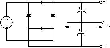
I found this page on split power supplies that seems to have a simple circuit recommendation.
That square of diodes looks similar to a bridge rectifier which I understand converts AC to DC. Is this what you meant by a split power supply?
Hi Pix
That IS a bridge rectifier and that IS a split power supply.
That is not what I meant by “artificial analog ground”. That is achieved with 2 resistors in series between VCC and ground. The “Analog Ground” point being the junction of the 2 resistors which would be VCC/2. Value is not critical, 10kΩ being a popular choice. This has the effect of level shifting the “analog ground” by VCC/2 which in your case is 2.5V. Thus subsequent audio amps see the signal as being +/- WRT VCC/2 and operate with a single supply.
A nicer way of doing this is to apply this junction (2.5V) to an Op amp non inverting input wired as a voltage follower and consider the Op amp output as the “Analog Ground” point. This will provide a low impedance “ground” if that is required.
I will reverse that upper amp input connections and run the simulator again when I get a moment to spare.
Cheers Bob
Hi Pix
Have reversed Op amp connections and run simulator again.
200mV P-P input
1V P-P input
2V P-P input
The ground reference is the same for both traces. Note if you look carefully it is 2 divisions below the centre of screen.
Now I don’t know what you are trying to do here so I will leave you with these results. It still looks like a switch or the Op amp is just being driven to cut off in both directions.
Suggestion. If you just want to keep audio at a constant level I would suggest you have a look at a device I came across while contracting to GEC Marconi some 25 years ago called a “Compandor”. I don’t remember all the details now but there were time constants involved to prevent modulation being wiped completely due to the device fast action
Cheers Bob
Lot’s to think about there. I’ll take your advice and reverse the OpAmp. I’m not sure it matters for my ADC but it’s certainly more intuitive to think about your way.
I’ll also throw in the bridge rectifier. That’s a good idea @Robert93820 . Thanks so much; I really appreciate your experienced advice.
I believe this circuit will oscillate faster when the frequency of the sine wave increases. We will find out
You are right and I think you should start doing it. It is still unclear (to me anyway) exactly what you are trying to do with these 2 Op amps. If you are trying to get a constant output level with varying input levels you will find this a bit more complicated than first meets the eye. I had a quick Google and this can get quite complex. You are effectively removing the dynamic range of the audio signal and would sound pretty terrible.
I had the idea that an ADC resulted in a number relative to the Amplitude of the input, not the frequency. Could be wrong.
Just where did you plan on “throwing” this. That circuit you posted is a “split” power supply sure but is usually driven with a transformer. I have no idea what that circular thing is. It is marked “S” and “G” which just confuses the issue. You can’t just “throw” things like that anywhere and finish up with a “split” supply. I only mentioned this as a lot of circuits require this and if as I said you are applying a “true” AC audio signal to a single supply amplifier you have to level shift the audio to VCC/2.
The LM358 is described as a single supply amplifier. Now this may not suit split supply. While split supply amps can mostly operate from a single supply by doing the level shifting the opposite is not always true. Depends a bit on the output configuration I think. So your LM358 may not function with a split supply.
Just quickly checked. TI and OnSemi data indicates this will operate with a split (+/-) supply.
Of course it will. The 555 will probably be triggered with the audio signal if it is large enough.
Getting back to your Op amps. Basically as you have drawn it with all the positive feedback I think it is just a switch which you could have done with a Schmidt trigger. But by changing the feedback circuitry to negative feedback it just becomes an inverting amplifier. I think you should do some reading re what you are trying to do. If it is as I suspect above this will involve signal rectification and some processing to supply an automatic gain control of an amplifier. Getting a bit confused actually.
Cheers Bob
Oh I see you meant the Op Amps specifically.
For clarity, the OP amps are the to regulate the voltage precisely so the audio signal large enough to drive the NE555. Here is the schematic I’m following
Ah this helps clarify the why of the split power supply. That’s super helpful. I need to bring the wave up to half of the voltage of the circuit.
I’m actually not sure yet. I think I’ll need to build it first to really understand what your communicating. I don’t have enough experience to be able to predict what a circuit will do. I might have to jump in and try some stuff to learn.
Hi Pix Here is the schematic I’m following
Here is the schematic YOU DID NOT follow. Your original has pins 5 & 6 reversed to this. That is the positive feed back I questioned. And I suggested these 2 connections should be reversed which the circuit you linked verified.
That Op amp is configured as a non inverting voltage follower and will present a very high impedance to the charging capacitor C2 so as not to affect it. This is then in a POSITIVE feed back loop for the bottom amp. In isolation (as I simulated it) this then will be a switch. I think the author has designed a constant current source to charge C2. Without this the charge across C@ would be non linear and he has achieved a linear result using the Op amps.
Having a quick look at that article I think he is after a frequency to voltage converter or something. I am not going to try to guess exactly his intensions are so all I can suggest is you build up the circuit CORRECTLY as published in that article and see if it meets your requirements.
Don’t throw a bridge rectifier anywhere unless you are building a power supply from scratch and don’t worry about level shifting the audio at this stage. I think that author tested with a variable DC voltage and that is how he got the C2 charge plot.
Cheers Bob
Ah! Good catch! Pins 5 and 6 are backwards! Thankyou
Your simulations seemed to produced outputs that looked like they would work too. I wonder how this will change the output of the 555 timer.
I think audio is AC. Wouldn’t I need some kind of AC to DC converter somewhere in this chain? I don’t think a 555 timer would no what to do with AC.
Once it leaves the Op amp it won’t be AC. It will probably be switched DC. Bear in mind the cap C2 was not included in the simulations. With this in circuit and the means to discharge it you would probably have the sawtooth waveforms shown in that link.
Hi @James.
I did think about latches and JK flip flops.
I could use the fact that they typically have a Q and ~Q output to toggle the outs in the right way.
However having thought it through this week I think this would require two clock pulses and I only have one to work with.
I think I want to make a video over the weekend talking through my diagram. There is so much going on. First, however, I want to add in Roberts suggestions and correct the flipped pin 5&6 on the opamps.
It may be that the answer here is a ATiny85 microcontroller listening for a hardware interrupt.
I had dreams of using no C++ in the project but that was just to force me to learn new skills.
“Better to finish a compromised vision than for it to remain merely a vision.”
Sun Tzu in colaboration with Jesus of Nazareth 420bce (probably)
I note the plural “opamps” There is only one with pins 5 & 6, the top one in your diagram. That was something that stuck out as being funny on your first schematic. You would not have positive feedback in that configuration. Swapping YOUR connections just brings it in line with the original author’s schematic.
I was correcting an error on your part.
Cheers Bob
The IC I’m using is the LM358. It’s just a dual Op AMP. The default version of this in Kicad splits the OPamps in twain, giving two separate symbols. I assume that’s just convention.
I must have made a typo when I was modifying which pin goes where. Maybe in my updated version I should create a new Symbol in KiCad that renders the LM358 as an IC with all the pins as below.