Hey all,
Is there a ‘best practice’ tute somewhere about PCB layout using SMT devices. I’ve done numerous through hole layouts but surface mount is a whole new ball game for me.
Cheers,
Gerard
Hey all,
Is there a ‘best practice’ tute somewhere about PCB layout using SMT devices. I’ve done numerous through hole layouts but surface mount is a whole new ball game for me.
Cheers,
Gerard
Hey Gerard,
I’ve done a little work in KiCad, and the process for SMT and THT isn’t too different, just smaller components so you can get things really close if you need to.
KiCad will give you a “net” with lines drawn for all the connections that need to be made, so I usually just rotate (R key I believe) and move the components around such that there are a reasonably small number of overlaps or unnecessarily long traces.

(This isn’t one of my designs, just a good example of a complex net)
My designs are pretty rudimentary and low-frequency for now, so I don’t need to worry too much about the effects of my layout, things get a lot weirder once you get into high data rates or RF.
Perhaps @Rob110829 Has some words on this one?
-James
The basic techniques are the same, try to keep vertical tracks on one side and horizontal on the other. Flaunt that rule too much and you will be in a world of hurt.
That said with 4-layer boards being so common now I tend to take a few liberties with that rule, especially towards the end of the routing.
One “problem” though is that because everything is smaller you tend to make a smaller PCB, trouble is there are still the same number of tracks to be laid with only (for example) half the real estate to work with, that can make life difficult to impossible even with 4 layers. I was tempted to go to 6 layers recently but the cost is prohibitive really.
Here is the layout for the first version of my QUUB design
I probably spent a couple of days routing the final 10 tracks 
On the plus side, as mentioned, we now have ready access to 4 layers. I would never dream of doing a 2-layer board again. One of the HUGE advantages of 4 layers is that you can almost forget about GND and VCC tracks, these have to be thick and are often a nightmare with two layers because they themselves can take up half the real estate. With four layers you can simply make the inner two as planes connected to GND and VCC and pretty much forget about them.
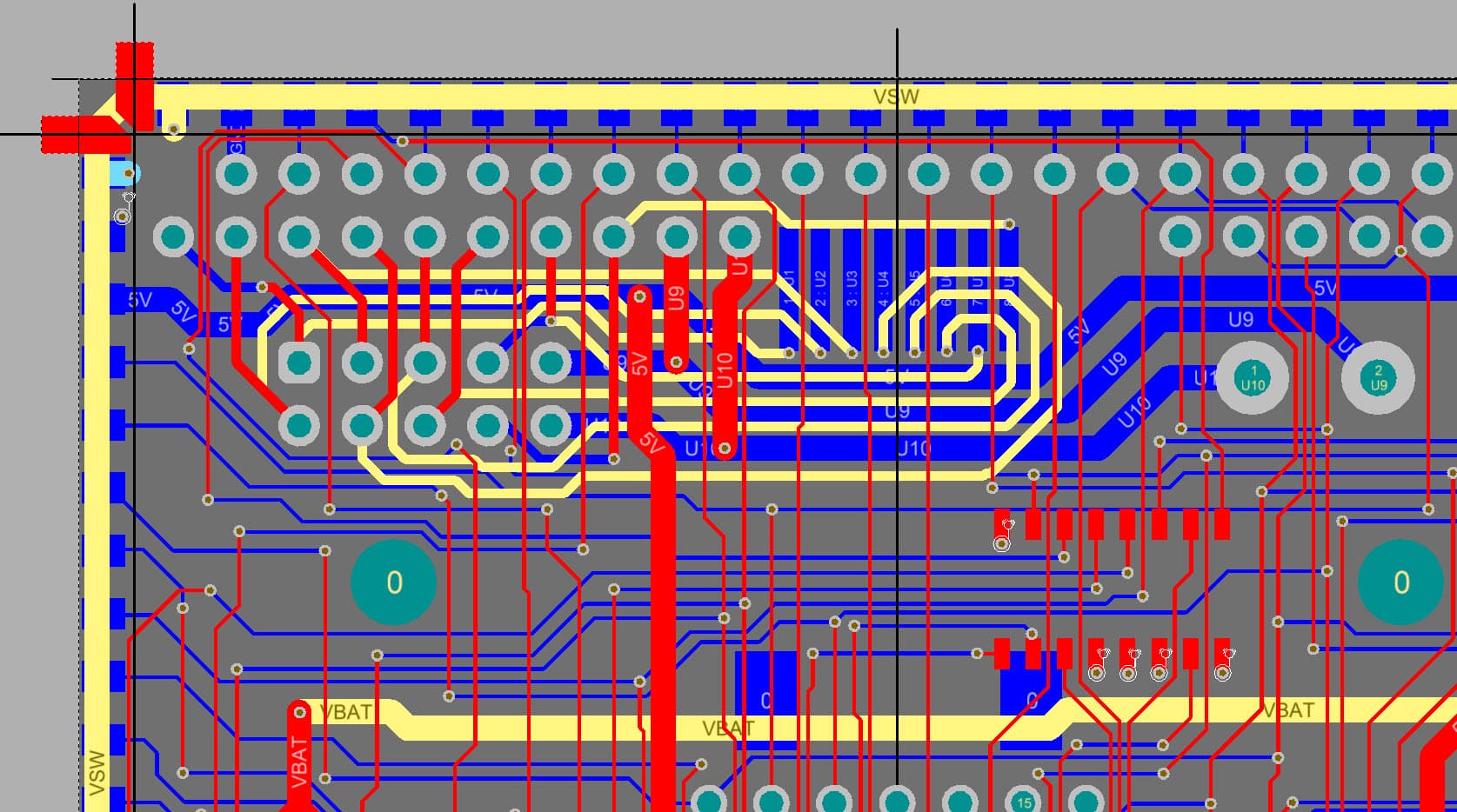
However I do often run signals on the inner layers as well, you can see some on the above layout but they are clearer on this one (the latest QUUB)
Those thick yellow traces are on an internal layer. Ten minutes work that would probably have taken days if I restricted myself to the top and bottom layers. Note however that the majority of the signals are on the top and bottom and pretty strictly conform to horizontal on one side and vertical on the other.
Another obvious advantage to SMD is that you can have components on both sides, I often do this for decoupling caps, especially with CPUs that need 4 or 5 of them, but I try not to put much on the other side, it can really do your head in.
Hi Gerard,
As James mentioned most of the same rules apply:
Another great place to learn is YouTube (A great mechatronics channel I’ve been binging recently), open-source designs from wherever you can get layouts - Core’s GitHub, takeing a look through some of Pololu, Raspberry Pi Adafruit and Sparkfun’s designs, even some reference circuits for specific chips have SMT layouts.
When designing in general I like to make notes as close to the ‘decision’ as I can, eg the calculatrion to figure out resistor values will be on the schematic.
@Rob110829 got in before me, geez the detail on that board is next level, does the fab house that you use allow for blind vias? I’d imagine that would make design a whole lot easier.
Liam.
Yeah blind and buried vias would help, I’m not sure if the fab houses I’ve used allow that, probably, but it’ll cost more and you can get by without them.
Rob, what’s the difference between blind and buried vias?
Edit: Also, that’s a sweet piece of layout work. I try to keep my stuff pretty neat and tidy. I lay any busses first, then do the rest, finishing with pwr and gnd. As I said, my experience is through-hole but I must bite the bullet and do some surface mount.
Hi Gerard,
Blind and buried vias become are a type of via that can be used for multi-layer PCB’s Blind being ones that dont penetrate through all of the layers, and buried being ones that are on an internal layer. Have a look at the diagram JLC have

:
Many manufacturers include PCB layout guidelines in the data sheets for their chips, especially if the chips are at all sensitive to the correct layout, so it is worth looking at the datasheets for the chips you are using. In any case, it is worth checking in order to see what sorts of considerations they have mentioned in explaining their choices.
Thanks. Of course functionality is the important thing, but I also like to make the layout look good, things like the above are almost artwork eh? In fact I have hung this image in a gallery before
Rob
And you can get our latest projects and tips straight away by following us on:
![]()
![]()
![]()
![]()