I have progressed my prototype to the point of upgrading to a PCB… which I’ve never designed before, so have some noobie questions (and I’ve learned not to put too much store in chatGPT’s advice)
I am running a Pico 2W, and wireless comms is critical for my use case. I connect some sensors and several other I2C devices, eg a VL53L1x distance sensor, a Transceiver module, 3 x displays, plus I have a quad op-amp for some sensor signal processing before it is presented to the Pico.
Immediate questions:
Is there any good reason to put an ESD chip on the SCL and SDA I2C lines, ie between the Pico GPIOs and the Qwiic connector? My guess is “No”.
I have a ground plane on the base of my 2-layer PCB, and I suspect I need to customise it… to avoid the Pico W’s wireless keep-out area… please confirm.
Related to 2… I’ve seen a couple different versions of where the keep-out area actually is.
Try to avoid acute or “Y”-style joins where two traces meet at a single point. They can cause reliability, manufacturability, and electrical issues. A better approach is to route a single trunk and then branch off with 45° traces. You can see an example below, R7 has this as well:
In general, aim to keep traces as short and direct as possible, especially for high-speed signals.
Now, onto your questions:
You’re right, usually not needed if the I²C bus only stays on the board. If the Qwiic connector will be exposed to the outside world, then it’s worth considering a low-capacitance bidirectional TVS array or small ferrite bead on each line to help protect against surges.
Yes, you should leave a cutout in the copper pour under and around the Pico W’s antenna to avoid degrading wireless performance.
There isn’t one single published “official” dimension from Raspberry Pi. The optimal keep-out can vary with board and enclosure, but as a guide, page 27 of this document shows the recommended antenna cutout.
Add on to Ryan’s comments
C1, R5, D3, RV1, Pin 1 of U1 don’t appear to be on the same grid pattern. Is there any reason for this.
If Were doing this I would start with the 0.1" or 2.54mm grid. Get everything you can lined up with this including any board mounting holes. Then bring in a 1.27mm grid. Then if required the 0.635mm grid for the really difficult bits.
Then you will find you get rid of all the little kinks like around the C1, R5, D3 area.
Like Ryan says there is a bit of “fuzz” around R5 pads and also D3 as iff these points are going to connect to the ground plane. Which would happen if you etched from that art work.
Anyway, for a first attempt s pretty good. You will no doubt have a few failures before the final design.
Cheers Bob
Your top pic shows my 3.3V supply to the I2C Qwiic connector… I did the Y thing to avoid a right-angle, since I have it on good authority they are bad Not sure if this applies to power lines or only signal… ? I’ve re-routed the 3.3V line around the other side of the I2C connector now, which avoids the issue.
KiCAD thinks the trace from D3 to R5 is fine… albeit has a slight kink in it. I moved D3 a bit and eliminated the kink…
R7… you are right, I can and have improved this. Thanks for these tips!
The I2C connectors will connect external devices… some nearby inside my main enclosure (LCD displays and Tranceiver), but also my primary sensor… the VL53L1X which will be 500 mm away. This probably the only device which may from time to time be disconnected/reconnected.
Remaining questions:
The 4-way DIP switch next to my op-amp is to enable me the option of either grounding the inputs to units B & C… (I can thank Bob for this tip ) which will be the initial config… until I find I want to add something later… and I can connect +/- inputs via J14 or J15 and outputs via J16. Well, that is the plan… but it feels a little janky. Might there be a better solution? Cutable traces or something? Would be more compact!
At top left, I have a JST for connecting 5V external power, with a slide switch to throw if I connect a USB cable to the Pico. I have yet to resolve if/how to connect a LiPo and charging circuit, a’la what you guys have done on the PiicoDev Platform. Any ideas on this greatly appreciated!
@Robert93820 , not sure why things are not all aligned… I did not change any of the default grid settings… oh, just remembered… I have at times resorted to holding down the CTRL key to move things a little so they line up. Maybe that’s the issue… Bad Dog !!
@Ryan Yeah I looked at the datasheet… the weird thing is, the bit drawn (id’d as a cutout?) does not really line up with the physical position of the WiFi unit on the Pico itself. Go figure. I’ll probably just use what I have shown on my design as the blue-hatched area… to be safe, and see if it works!
Of greater importance to the operation of my widget is the performance of the PicoDev Transceiver… which talks to it’s twin connected to another slave unit Pico some meters away from the main unit - it is the slave device which actually controls my bore pump. Failure of this comms link represents failure of the entire system! And yes, I have code to detect this and take necessary action. (My total code for this project is around 4,000 lines of Python… and still growing!)
Hi Trevor
If you manipulate the grids as I suggest above, the component pads will snap to this grid.
Start with the 2.54mm grid then introduce the 1.27mm and 0.635mm as needed.
Aligning any mounting holes to the 2.54mm grid pattern will make it easier to mount this board on something else like a proto board or similar.
Cheers Bob
Ah… I didn’t check earlier, as I assumed out-of-the-box it would use standard 2.54 mm spacing. I just explored under preferences, and I see Grid 1 (the default ?) is set to 0.5 mm, Grid 2 to 0.25 mm.
This may explain why at times I resorted to CTRL key adjustments! Another lesson learned for a beginner KiCAD user!
I’ll set it up to use “normal” spacing… things might work better for me!
Hi Trevor
That’s interesting. I wonder they went away from the “standard” grid pattern. No wonder nothing lines up.. People these days even advertise that something is “breadboard compatible”. back n the days when things were “normal” this was automatically assumed. Nearly always correctly.
I have never used KiCad for PCB design. When I did a bit a few years ago I preferred Sprint Layout. An Abercom product.
Cheers Bob
Yeah… making progress… but slowly. There doesn’t seem to be a tool to make components snap to my new grid spacing of 2.54mm. This is proving to be a pain in the butt, and doing what I am doing will take forever to realign everything Grrr…
I read in a blog post somewhere a week or 2 back that the latest version of KiCAD changed this behaviour.
Reminder for next project: Get the grid setup right BEFORE you start placing things! Sigh…
Clicking on that bit on the right of the grid box brings up a drop down with grid selections from 12.7mm to 0.0254mm then 5mm to 0.01mm thus providing for the 2 systems.
The other is in “KiCad” options.
I click “KiCad” at the top.
I can assure you that when you select a COMPLETE component in PCB Edit mode and move it the pads WILL snap to the selected grid.
As I said I start with 2.54mm then work down from that. The smaller grids are useful when it comes to routing tracks.
Hope this helps.
Cheers Bob
I don’t know how this goes with mixed grids. Some connectors I think are based on 2.5mm and sub multiples of that and I think some surface mount components are the same.
I am a bit intrigued about that and will have a look when I get a bit more time.
I’m using v 9.0.4… the latest update. in PCB Editor, it now shows a drop-down which shows 0.127 mm (0.0050in)… and I changed the settings in Preferences to use the 2.54 stuff., plus, if I right-click on the PCB, it shows another drop-down list. On an older version, on a Mac, it may be different.
I also have (and have always had) Always Snap to Grid ON. If I now place new component on the board, it does the right thing… but the existing component positions remain on the old 1mm grid… and moving them, even with the new grid spacing, and Snap to Grid on… leaves them on exact 1mm grid positions, rather than moving to a 2.54 or 1.27 multiple position. That, or they move to arbitrary positions, rather like holding the CTRL key down (except I’m not…) Arggghhh ! And there’s why it looks grim.
Just had a thought…if I start a new board and just copy everything over… if that might result in correctly grid-aligned positions… I’m not experienced enough (obviously!) in KiCAD to know about this… “Start new board”… ? How?
Perhaps I need to delete everything on this board… and then re-add them?? That is still a fair bit of work… as I guess I’d lose all the traces.
Any pro KiCAD users out there care to provide some guidance?? I might ask on the KiCAD forum..
PS… I dropped the pull-up resistors I had cunningly placed near the I2C connectors, as I found just about everything I have connected has internal pull-ups… so I figured I really don’t need more!
EDIT: Found the KiCAD forum link that discusses this frustrating behaviour… so no, it’s not just my stupidity!! See here for full discussion
Strange. I have a project I started on and I just created a 2mm grid and moved a couple of connectors to that. Then I went back to 2.54 and moved them back again OK.
Like you said differ versions and different PCs seem to behave a bit differently.
One thing I like about the Mac though. At the moment I have a KiCad project open plus Safari with 13 tabs across the top, all available.
When I shut down all disappear of course and the machine turns off.
When I start up again to-morrow all Safari tabs reappear plus the KiCad project just as it was when I shut down. All very useful, especially Safari and all the tabs which are lots of data sheets and the Core shop part of the site and things I refer to through the day. In other words it starts exactly as it shut down.
I have another Windows lap top on the table as well but it does not want to do anything like that
Cheers Bob
I looked at the KiCAD nightly build downloads…but think I’ll wait for 9.0.5 release. I have enough headaches already, without creating new ones!
As for Mac vs WIndows… yeah. Mostly Mac stuff is great. I was one of the really early users… probably got a Mac before most people in the country - was working at the University at the time… but I digress.
On your Windows system, I use a package called Workona. Free (or it was when I first got it) As a browser extension, it does much the same as you describe happens on your Mac
I use Firefox, have about 70 tabs open (in multiple tab groups) and can instantly get them all back after a logout. Nice. I can’t give it a 10 out of 10… it does seem to have some glitches, but I’d be lost without it … so I keep using it.
Try it if you want a similar UX (at least regarding browser tabs…)
Hi Trevor
I think you might be referring to the Antenna area on the board.
I don’t know of any hard and fast rule regarding this but i haven’t done any detailed search either.
From what I know of RF I would suggest an area a bit larger than the area on the Pi. You don’t want it to be the same size or you might find a related resonance and the hole could become a “Slot” antenna in itself. Maybe an area as large as practical without going overboard.
IMPORTANT: If you have a double sided board remove ALL the copper in this area from BOTH sides. Don’t just hatch it as you suggest in your KiCad layout. I appreciate this layout is in very early stages but just thought I would mention it.
Cheers Bob
Sorry I have done it again. I did nor read post 4 properly.
Re power. I think a lot of bits have this taken care of in the shape of a diode (or 2) and maybe a Mosfet to arrange USB power priority when available, only falling back on external when USB disconnected. So depending on what your circuitry looks like this might be already done for you. I don’t have the time to research just at the moment but there has been some discussion re this in the past.
Re unused inputs and grounding DIP switch. Remember these inputs are very high impedance (10 TΩ) so any tracks hanging off them will be little antennas. If you want to bet rid of the switch I think solder pads adjacent to the pins that can be bridged to ground would be the go. I am assuming that this is a 2 sided board and the top copper plane is ground. With no switch you might be able to get J 14 and J 15 a bit closer to the pins too. The outputs (pins 7,8) are a bit more forgiving being low impedance.
Cheers Bob
You can definitely add a LiPo + charging circuit to your board via using the VSYS from the Pi Pico. The usual approach is to use a small LiPo charger IC (like the MCP73831) that takes in 5V from USB (VBUS) or your external supply and handles the battery charging current safely.
Here’s the basic flow, as done on the PiicoDev LiPo Expansion Board:
VUSB (USB 5V) feeds into the MCP73831 charger.
The LiPo battery connects to the charger’s VBAT pin (via a JST connector).
The charger’s output (the battery voltage) is then routed through a power-path MOSFET to the Pico’s VSYS pin.
The Pico automatically runs from USB when it’s plugged in, and falls back to the LiPo when USB is unplugged.
Since VSYS is available on the Pico header, you can also tap it with a simple resistor divider into an ADC pin to monitor battery level in software.
This way, when you connect the Pico over USB, not only does the board run normally, but the MCP73831 also charges your LiPo. When USB is disconnected, the Pico runs directly from the battery so no need for a manual switch.
@Robert93820 Bob, my ref to hatching only means that I show the keep-out area as a graphic in the PCB designer - nothing to do with actually laying down a hatch pattern of copper! I have drawn a larger area than was on the library part (shown as a smaller red hatched region). And I still have not modified the copper pour on the back… but it’s on the (long) to-do list!
@Ryan - thanks, I already looked at the LiPo Expansion board circuit many months agao I presume I could modify what you said about the USB 5V supply to actually connect where I have my external 5V coming in. (Sorry, I probably should have attached my KiCAD schematic so it’s easier for others to follow… I’ll do that today. )
My thinking is that this will be the “normal” (and always-on) state of affairs… I only expect to connect a USB rarely and short-term, for the odd maintenance operation etc, in which case I really don’t care about the LiPo being charged Thanks for the ref to MCP73831 however… I don’t see that on the schematic.
Which still leaves my query about replacing the 4xDIP switch with something else… which is in the top left of my schematic.
Hi Trevor
I think our posts crossed paths. I have since added to my reply above concerning the DIP switch. You may not have seen this addition.
Yes the schematic does make things a bit easier.
Cheers Bob
Yeah, you definitely can. You could even wire it up like in the diagram below, with your external 5V and VUSB each feeding through a fast switching Schottkys diode into the same node. In this case the “load” would just be the input pin for the MCP73831. That way it acts as a diode-OR configuration, whichever supply has the higher voltage will win, and you can completely drop the physical switch.
The last revision of the board looks to be from 2021, when power ICs were really tough to source due to covid shutting down a lot of manufacturers. A lot of teams (including mine at my previous job) avoided putting the exact part number directly on the schematic, instead just listing it in the BOM. That way you didn’t have to keep revising the schematic every time you had to swap to a like‑for‑like part during those shortages.
Or, of course, it could simply be that the identifier was forgotten to be placed
Either way, the original designer was thoughtful enough to include the datasheet in the GitHub repo, so we can still trace exactly what was used.
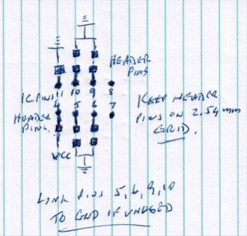
Fit header pins as shown. Keep everything on the 2.54mm grid. If the inputs are not used you can use the small shorting push on links to connect them directly to ground. Or if used you can use the pin to connect to the outside world. The ground pin is there if required.
If, as is often the case, there are components associated with the use of an input they could easily be mounted on a small Daughter board. You could even use a bit of photo board as (hopefully) all these pin connections will be on the 2.54mm grid. I suggest a header pin on the indicated positions for Gnd and Vcc for this purpose in case this is required.
Cheers Bob
Core stock these small links. They call them “Jumper Shunts With Handle” SKU ADA3525.
You can omit J14 and J15 and use these header pins to connect.