I like it, Bob! so much better than my “solution”!
And thanks @Ryan for your comments above - also a great improvement on my amateur-hour design ;-). Looks like I’ll be doing a major rev to that PCB layout… better now than after I’ve had it made!
You can say that again.
If you still can’t get your component footprints and pads to lock to the 2.54mm (and sub multiple) grids you might have to start again. Might be the quickest anyway.
Cheers Bob.
Happy to help! Much more enjoyable reviewing your board than the ole mining projects I was involved with
And nice suggestion from Bob about using header pins and jumper shunts, that’s a tidy way to keep things flexible without needing the DIP switch footprint.
If you have some extra time on your hands, have a play with adding a custom logo to the board. We’d usually hide these under the main MCU as our own little calling cards I’m not too well versed with Kicad, but the guide I linked seems straightforward enough.
Well I’ve been working on the new schematic & PCB layout… until 3:30 AM ;-( I have most things in place, (using SMD not THT) but I’ve screwed up something (confusion between VBUS and VCC) My head hurts…will continue tomorrow!
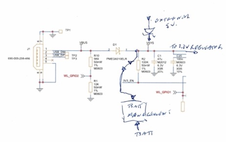
One last query re the LiPo charger… I’ve dropped in a MCP73831, and back-to-back Schotttky… Does the Schottky mean I don’t need the MOSFET shown in the PiicoDev Platform circuit?
I’ll attach updated schematic and PCB tomorrow… after I fix the remaining power issues.
Just a minor comment - many of the traces are quite narrow. If there is no reason for them to be that narrow, I’d make them wider. You pay for the copper, might as well use it.
@Alan73922 maybe many of the traces look thin in comparison to my beefed-up 5/3.3V traces… I made 5V 0.8mm wide, most signal traces were left at the default. Happy to change these… as I just a beginner, with zero experience designing PCB’s !!
@Ryan Well. I am now quite confused (sleeping helped a bit…but not enough, it seems!)
My original schematic had a notional VCC net… seemed a good idea when I started this exercise, but that’s now gone, after trying to add the LiPo charging circuit. I think after re-reading the Pico datasheet that I should be connecting the various other bits (eg op-amps, sensors etc) to VSYS, not VBUS, and I tried changing my schematic accordingly, but am now hit with a few brick walls:
I can’t run a trace from Pico Pin39 to my VSYS net. KiCAD insistes Pin 39 is in fact “A1-VSYS”, so wont connect to anything I’ve labelled as plain old “VSYS” in my schematic. OK.. different nets - I get it. Does this imply my schematic VSYS labels should just be changed to “A1-VSYS”? (Most of these were previously designated as VBUS… after I changed from VCC… if that makes sense)
My little far-right of page thing that shows C2 and power connection to my op-amp… KiCAD doesn’t like this either. Got power inputs/outputs mixed up… OK, I get it, so what should I have on pin 4 of U1 (op-amp)
LiPO charger, external power input & Schottkies… This seemed straightforward, but clearly I have screwed it up, and my circiut is now a nonsense. I need help to unscramble the mess I have created ! D’oh !!
Bob, I told you I was more a programmer than an electronics engineer… this proves it!
Positive supply as shown in your schematic as U1E. That agrees with the data sheet for the LMC6484 which I just checked.
Pin 11 is ground.
Cheers Bob
You have this marked as "VSYS which could have something to do with it.
There looks to be something wrong with that power arrangement . The output of the chip will go nowhere. The diodes will see to that. The 2 supplies via the diodes seem to only go to the chip output so I think something is not quite right here. I think there should be some sort of flag here.
I just noticed you do have “PWR_FLAG” hanging off this point (whatever that is) which also appears at pin 39 which you also have VSYS TP. Something not quite right and I don’t have time just now to investigate.
Go to bed for a good night’s sleep and attack it with a clear head tomorrow.
Edit. I incorrectly said LMC6482 above. Have corrected to LMC6484
Yeah that’s right… I know. The issue is how to enter this into KiCAD without it having a dummy-spit.
I might just change my VSYS flags to A1-VSYS, but honestly, I got tired of the “Let’s just change this and see if it works” approach… was hoping wiser heads could advise the correct way to do it, and that would be it!
The multiple power source stuff, MOSFET’s etc as described in the Pico Datasheet… makes sense to me, but I feel I’m somewhere in no-mans-land between the Datasheet circuit and Ryan’s suggestion with the dual schottkys, and my attempts to reconcile the two have not gone too well. Dang…
Thanks to all who are trying to help me sort this.
Hi Trevor.
Just noticed there seems to be another diode as part of the Pi which connects VBUS (pin 40) to VSYS if it is forward biased. A bit confusing.
Cheers Bob
Hi Trevor.
Just had a quick look. And I stress the word quick.
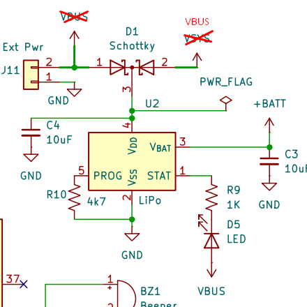
Your external power is going to the wrong place. It will back feed into the USB port the way it is.
The diode from VBUS already exists on the Pico board as “D1”
I found what I think is the correct schematic for your Pico and extracted the relevant power input bit. I have indicated where I believe the external power input should be with a series schottky when the USB AND external power is connected the highest value of the 2 will win. That should not matter. Sketch follows
The yellow box with the battery connection is a mystery to me. I am not sure what it is and what it does. I assume it is some battery management system. I have just drawn a box and called it “Battery Management” for want of something better. Will leave that to you.
I have marked this box connection with a couple of arrows. They are not diodes. Merely signifies 2 way traffic, supply and charge. I am assuming that is what the battery management device has to do.
I will be away this weekend so will not be around until Sun PM or Mon AM.
Cheers Bob
PS: Your LMC6484 power (pin 4) should connect to the point marked “VSYS” in the above sketch. Assuming you are powering with 5V.
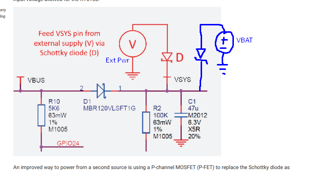
In that setup, VBAT ends up simultaneously powering VSYS and its own charging circuit, which creates a feedback loop. That can cause problems since the system is essentially trying to charge the battery from itself.
Now, whenever VBUS or the external supply are present, the battery gets charged. When they’re not, VBAT can safely supply VSYS without that circular dependency.
The next question is how to decide which source powers VSYS at any given moment. Section 4.5 Powering Pico of the datasheet explains how the Pico handles this. Your design is slightly more complex since you have three possible sources, but the same principles apply.
One straightforward option is to use Schottky diodes like this:
Referring to the first schematic.
How is the battery going to do that while there is a diode (Pin 2 of the dual schottky) in the way. Don’t forget “VSYS” goes to the 3.3V regulator.
2nd schematic.
Ca’t see how that is going to happen either
3rd schematic
How is the battery going to charge. There is a diode in the way.
4th schematic
Once again how is the battery going to charge.
Going back
Isn’t there something in the battery management box which prevent this. That is while there is USB or external 5V present it charges and only SUPPLIES power (5V) when either sources are unavailable. I thought that was the whole idea of these ICs or modules.
I think there is some sort of a mix up here. According to the Pico 2W schematic I am looking at there is already a schottky diode between the USB supply and the rest (D1). Including the pin marked VSYS. Any external supply has to be connected here (VSYS) preferably via a diode if there ai any chance of external and USB supplies being connected at the same time.
The connection between VSYS and battery management has to be 2 way if charging is required.
That battery management IC type is not clear as it is not shown on Trevor’s schematic. It is probably stated in the post text somewhere but I have not the time to search for it. If Trevor can’t get anything better than “Lipo” on the schematic it can remain a yellow box mystery.
Cheers Bob
Thanks to both of you for persisting with me on this…
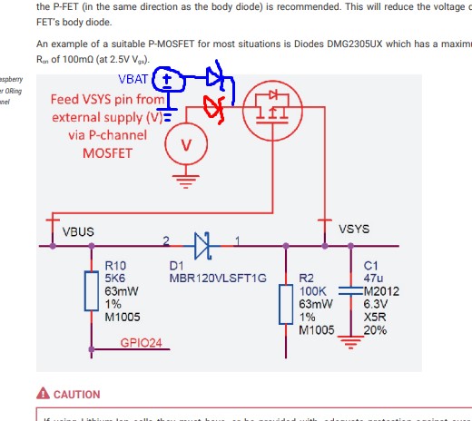
Over the weekend I thought it might be best to just use the battery chargiung circuit shown in the Pico Datasheet… which I’ve now included, and replaced Ryans back-to-back Schottky’s with a MOSFET, which seemed to be the “preferred” solution.
@Robert93820 the charge management IC is an MCP73831… same as Core used in their PiicoDev Platform. Sorry, part id was too long to the silkscreen, so I shortened it to LiPo. I’ve now added this on the schematic. Ditto for MOSFET… it is a DMG2301L
I hope I have the MOSFET connected correctly… don’t assume I have!
So I understand VBUS on the Pico is connected to the USB 5V.
I had some battles with KiCAD regarding VSYS, now sorted, I might return to this later… for now, it is sorted, mainly after I renamed my VCC net to VDD.
So the rmaining issue is to ensure this 3-way source of power does what is hoped. And I thank you for helping with this… as my brain was exploding late last week!
Mine is exploding now.
Let’s take this apart.
You have VBUS now called VDD which in turn is connected to USB as part of the Pico, You can’t change that.
This then becomes VSYS via Pico diode D1, You can’t change that either.
You then have External power (5V) connected to VSYS via Mosfet. That is OK as far as it goes. Whether the Mosfet will turn on is immaterial at this stage as the body diode will be ON if external power is present without USB power and you might just as well use have a diode here
You also have the batt management O/P connected to VDD/VBUS/USB. This means you can only charge when USB power is available as "EXT Power is prevented from charging by the Pico diode D1.
I personally think you are going in circles and need to sit down with the Pico power input bit and rethink the whole thing.
I will have a look at the info re that MCP3831 later today if I get a chance and see exactly what it is supposed to do. But at the moment I am a bit lost.
Cheers Bob
I guess I am trying to incorporate both sections 5.5 and 5.6 from the Pico datasheet, not sure this makes sense to try.
I will try to get my head around your comments above. I guess when Core designed the LiPo charge circuit for their platform, it was intended that the LiPo charger only worked if/when a USB cable was connected. Makes sense. So I am trying to mimic that so it works if External Power is connected. As I think I said earlier, I really don’t care if the LiPo is NOT charged when the USB is connected, as I only expect that to be for short-term maintenance operations.
That, I suspect, is a significant departure from Core’s use of the MCP73831, and might dictate a revision to my circuit ??
BTW… learned a useful tip re KiCAD doing this… those text annotations I added to the schematic, you can actually embed a URL with the text. So from within the KiCAD schematic editor, I can now directly open the relevant datasheet for the component. Nice…
Apologies was in a rush so couldn’t spend time drawing the whole charge circuit for VBAT in my drawings above. Piecing together my hastily drawn images, the circuit looks like this.
When VBUS or Ext Pwr are connected, they’ll charge the battery and power VSYS. If either become disconnected, VBAT will power VSYS. With the option to use a MOSFET configuration for choosing whether VBAT or Ext Pwr is used.
Its looking better, but currently looks like “BATT+” isn’t connected to VSYS in anyway. I’ve drawn a bit of a better circuit configuration in my reply to Bob above that hopefully makes sense
You can go with the MOSFET option, it’d look something like this:
I think I will leave any words of wisdom out until I have had a look at data sheets in future
I was assuming (Due to not knowing what that yellow box (Lipo) was) that this battery manager was a charge/supply device. I have since discovered (n looking at the data sheet) it is a charge only controller.
That of course changes nearly everything. The one thing that stands out is if you fall back to battery only operation you will only be able to power 3.3V devices and any 5V devices will be unpowered. VSYS feeds straight to a 3.3V regulator for everything Pico.
Ryan: That last little circuit would work OK if the drain and source are reversed. When the gate is grounded the Mosfet will be ON. If you connect the Gate (marked VDD) to VBUS (USP Power) the Mosfet will turn off when USB power applied. Thus isolating both Ext Pwr and Batt Pwr. The remark re 5V devices still applies, if both USB and Ext sources are removed VSS will only have battery voltage minus the diode drop at this point.
In reality I don’t think all this is as easy as it first looks. There are obstacles whichever way you turn. I do believe we are all going in circles in some respects. It would I think be far easier to have a battery backed up 5V supply as the external source and simply feed that into VSS via a diode. All done then. The way we are going most of the available voltage will be soaked up in diode drops. They all add up unfortunately.
Cheers Bob
Add ON:::
For what it is worth if you connect the Mosfet as I described above (reversing Source and Drain then connecting Gate to VBUS leaving 100k R as it is) you could do without that diode in series with Ext Pwr. The Mosfet is doing that job. The diode in series with Batt is still required
OMG… little did I realise I had opened such a can of worms! I apologise… and thank you both again, as there are clearly more issues here than I would have ever been able to resolve by myself.
I think it might be wise to pause and reconsider the whole thing. It seemed to me to be a spiffy idea to include a LiPo in my widget, so it kept running through minor power outages. It also seemed a decent idea to have a separate 5V supply, rather than a USB plugpack thing, and that would free up the USB port on the Pico. Considering all the above discussion, I am now seriously wondering if I just made a rod for my own back.
My prototype is sitting on a Core PicoDev platform… with the inbuilt LiPo charger, and connected via the Pico’s USB port. Perhaps I should simply replicate that… and call it a day? I mean… it’s a pump controller, not a life-support system! Heck, for that matter, I could even drop the LiPo altogether! If it reboots… so be it. I do like to do a “proper job” if I’m going to do something, but this feels like too much pain for relatively little gain..
Many thanks for your continued support… I’d be toast without it! On the upside, I sure learned a lot about KiCAD along the journey this last week or so.