
1 Like
Hey, Pixmusix,
I think it honestly depends on who your audience is.
I know with electronics schematics, you don’t need to show the Ground connecting back to microcontroller, just have it trailing off like so:
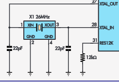
However, Voltage Input lines are usually drawn connecting like in this circuit diagram from Silicon Chip magazine:


Now, that’s clear to an electrician or a well-seasoned hobbyist, but if you’re expecting a newbie who has maybe only a couple of projects under their belt, that can be very confusing.
If your project is directed to the newcomer, t’s probably best to go extremely literal with what you’re designing, diagramming the literal layout of your circuit, such as this below:

In the end, your presentation really does depend on who you’re engaging with.
1 Like
Cool ![]()
So it’s a sensible option, but not always the best option. ![]()
Thanks Jane.
Hi Jane
Yes Silicon Chip schematics might look a bit congested at times but at least you are able to find your way around them.
I get quite annoyed at the latest trend (by so called experts) of filling up the sheet with little labels. “3.3V” or similar and the different ground or earth symbols are fair enough but others appear with no indication of where the other end is or indeed how many connections there are. Many years ago if this sort of thing was necessary there would be an arrow which if followed would lead one to the other connection for that net.
Another alternative which would be a big help would be to append a number to a label indicating how many connections in the schematic there are to that point. For instance if it were the number “2” you would know there was 1 other point with that label. If it were say “5” and you could only locate 3 others (total 4) you would know immediately you had missed one.
At the moment a lot of the KiCad schematics presented are pretty meaningless except to the author. If you are really interested you could spend quite a lot of time and still not be sure you have it all. I lose interest pretty quickly particularly if there is no valid reason for using such a system except to be an attempt to make it look professional (which it doesn’t)
If I do happen to get interested I use coloured pencils to mark pertinent nets.
Cheers Bob
1 Like
Hello all,
The silicon chip schematic is a good process to communicate through a schematic. They have been doing it to a standard for 30 to 40 years.
The rpi representation is a wiring connection picture not a schematic.
Also suggest if your schematic has a component in a location that requires 3v3 dont be afraid to just show the supply to it as a vertical line connected to a horizontal bar labelled 3v3.
Bryan
Ntat
2 Likes
Hi Bryan
I think it is called “Fritzing” whatever that is. I have not delved into this as I much prefer schematics.
Way back to “Radio and Hobbies” days when this was done by specialists draughtsmen well before PCs became the popular norm. The company I worked for (AWA) had such specialist draughtsmen who produced the schematics on transparencies for the printing process at the time.
I forgot to mention in this snippet of info
that the target point would also have an arrow pointing back to its mate to make the connection easy to follow. That is going back a lot of years now.
Cheers Bob
I am convinced, Fritzing is certainly the way forward for this hobbyist process of support as the circuits are not that complicated. The learner can see exactly what he/she or is it she/he must connect to achieve a result. Who are we from the past to advise/mentor at this level.
Good love to all hobbyist and enjoy.
Bryan
Hi Bryan
At least “we from the past” usually started at the bottom with some basics. It seems that an unfortunate trait these days with a good percentage of newcomers want to start half way up the tree. I am afraid I am not a big fan of that (my opinion only) and I believe a bit of time spent at the beginning on getting your head around some of the rudimentary things (like Volts, Amps and resistance to name some) will save a lot of hair pulling and make understanding a lot easier and more pleasant in the future. Does not have to go into the finer details of what is happening but even a general idea would often be sufficient.
I have worked on the idea that if I come across something a bit too complicated for my old brain and someone on a much higher pay grade tells me that if you do X then Y will happen I believe them. If I need to know why or how I can always find out later by asking the right people.
Having got off my soap box I will have a further look at “Fritzing”
When I first looked this was very much in its infancy and I was not totally impressed. It seems have gained momentum and popularity over time so it could be a good idea to re visit which I will do in the near future. If it is still like the pic Jane posted above there is still a bit to do. For instance those potentiometers. When you turn clockwise which way does the slider go? Towards +V or towards ground. Depends on which side of the pot the connections are. Top when looking down or bottom. Not obvious from that diagram whereas a schematic would have an arrow indicating clockwise rotation.
Just a little thing I suppose but could be important to someone new to this subject when everything seems to be reversed.
Cheers and I repeat your saying
Bob
1 Like
Hi all,
Just popping into this post - while not having read every reply. I find the best way to communicate this is through placement rather than labelling.
I couldnt find the exact video from Phil’s lab… but in more complex schematics its best to have inputs on the left, outputs on the right.
Generally, power being the first ‘block’ in that flow.
In KiCAD the net highlighting tool can show all connections either in the schematic or PCB editor.
Liam
1 Like