@Michael99645 , Yes the level shifter is bidi. It’s a TXS0108EPWR
I had to give it away for a day as it was doing my head in. Sometimes, you need to step back from a problem.
As @Robert93820 said, it could be a case of the camel’s back.
Actually, I only need 2 x soil sensors not 4 so maybe I can reduce the loading.
I have 2 schools of thought, one is that the overall capacitance ends up exceeding the ability of the supply (5v or 3v3) and the other is some kind of crosstalk creeping in. One of the keys is that it works much better with very short leads.
I also implemented the analog soil moisture design that @Robert93820 kindly did for me some months ago so that’s also a fall back position.
I’ll come back here later today and compare notes. I very much appreciate the input from all of the Core Forum people!
[ Edit: One thing I discovered is that the Arduino IDE will not change the clock for I2C (wire.setClock(xxxx)) even though when you do a getClock it reports that it’s changed the clock speed, but the scope still shows the SCL at 100KHz. However, using the ESP dev environment does alter the clock. Something about the Arduino IDE. ]
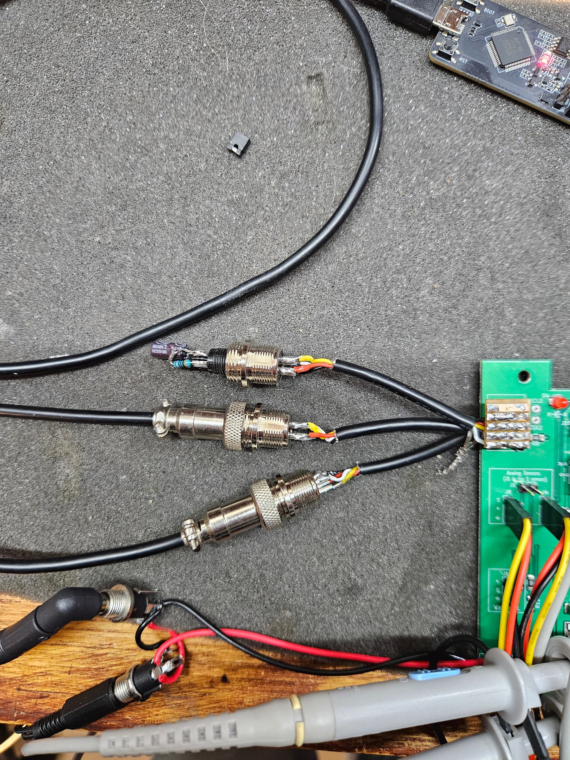
Here, I have cut the I2C backplane down to 2 GX connectors and have a female header straight onto the 3v3 powered I2C. Off that is an Adafruit moisture sensor on a 1m long lead and the HDC302x temp/hum sensor off a 250mm short lead. This works great.
The I2C backplane has traces that are 90mm long (both SDA and SCL) so maybe it’s acting like an antenna. That plus the (probable) capacitance challenges. See below…
Maybe, but what is it picking up ? If you can find the source of the noise, then may be able to work out the best way to deal with it.
e.g. Is the power management creating noise somewhere.
Is the ground plan running under the I2C traces or is their some other trace running in parallel on the underside of the board (or a different layer, without a ground plane between it.)
With the i2c bus, I see the capacitance as something that would make it harder to pull down the line at the frequency/speed selected i.e. more power to drain. This would show up on the scope as a “held high/slower drop to ground”, but the earlier images showed what seemed to be something oscillating. To oscillate something needs to charge and discharge at the measured rate.
So to re-group a bit.
WIth the nice clean 2 sensor setup, does it work well with all combinations of the sensors you have.
e.g. If you have 4 sensors A, B, C and D, does ir work ok with
AB, AC, AD, BC, BD, CD
Long I2C runs (like 1m) plus multiple devices can definitely cause signal integrity issues. Stronger pull-ups sometimes help, but usually you’ll need an I2C buffer/driver (e.g. PCA9615, P82B96, etc.) to keep the bus stable over that distance. Another option is lowering the I2C clock speed if you haven’t tried that yet. Given your setup, adding a proper bus extender between the ESP32 and devices will likely solve it.
Sorry for being late to the party, I wanted to do some tests to make sure.
I have used ESP32-C3 for this test but other devices have worked in the past.
I have four I2C devices (not the soil moisture probes you use - I wasn’t sure on the use of I2C) on 4 lengths of cable from 1m to 3m connected in a star network. The wire I tested with is standard CAT5 but I normally use Mylar shielded twisted pair (2 pairs) for outside installations.
I have no issues with I2C @ 100kHz - but I had to decrease the PullUp resistors on my CPU side to 1k (from 10k).
I’m sure you should be able to achieve the same results?
Hi Michael
You missed one, CD.
I also thought of that yesterday but I thought surely this would have been tried as Gerard had come up with a number. 2 items OK, 3 items no good.
But would be a big help to clarify.
Cheers Bob
Hi Gerard
I think what the measurements with different combinations is to determine if it is a definite device causing the problem or a loading situation where any 2 devices are OK and adding any one as a third device causes the upset.
If it is your power source getting close to breaking point it is quite possible the supply could be oscillating ie; switching on and off rapidly which looks like “noise” with your oscilloscope measurement.
It might a help if we could get an oscilloscope. pic of what that “noise” actually is. This might entail a delayed sweep measurement if your oscilloscope has the capability. I would be surprised if it did not. Are you familiar with this type of measurement. As different instruments have different methods of doing this it might entail a more thorough look at the manual. Most of the older analog instruments actually had 2 time base generators but the digital types do things a bit differently.
Anyway it would do no harm to become a bit familiar with this technique as it can be very useful.
Cheers Bob
There should also be a way to extract the screen shot as a file to a USB stick which will show oscilloscope settings a bit clearer so it all means something. These settings are not very clear in the photos and without knowing the time base period and voltage levels it becomes that much harder.
What is the main power feed ? is that clean ?
I had a similar issue a while back with false triggers and it look like those thin spikes you have.
The noise was on the power output I had from a high current DC-DC converter.
In my case I did two things that helped (note this was not I2C, but some bus lines for a cascading shift registers.)
a terminating resistor on the bus lines to help drain the noise rather then reflect it. (But this may not be a good idea for I2C
on the output from the DC-DC converter I run the power wires (both GND and Vcc) via some ferrite. The ferrite should help suppress the spikes.
And the circuit linked is a bit confusing. It shows a 3.3V I2C AND a 5V I2C as if both were available. I am not sure as the schematic is not complete but maybe you can use the 3.3V OR the 5V versions BUT NOT BOTH at the same time. If both are available and all your sensors are the same why are you using a level converter. Why not just use the one that matches your sensors. The level converter will add another pull up. If the sensors have on board level converters to accommodate both systems you will have converters on converters with pull ups all over the place and confusion must reign somewhere.
I would suggest you sit back, sketch it all out on paper and see you have no conflicts and go from there.
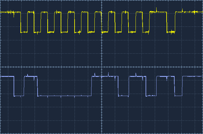
Regarding your latest screen pics. As they stand with the oscilloscope settings not visible they mean nothing. For instance what is the time per division, what is the amplitude volts per division, where are the ground points, where is the trigger position, is the trigger slope rising or falling. All this is around the edge of the screen but not visible in the pics. As before we know that yellow is the clock and blue is the data but besides seeing the relationship that is all. A picture showing all the mess when the system is not working might yield some clues.
Cheers Bob
Closer look, most of the spikes are on an rise or fall edge of one of the lines.
see green lines I added to better align.
So thinking a bit more, we have some pull up resistors allowing both lines to set at a “stable” +V.
We then pull down the line to bring it low and stop pulling down to let it rise back to +V for a high.
So when the data line pulled it down, it looks like its starving the +V a little thus a drop on the clock, until it recovers. then the 2nd green line shows a rise on the data line as the clock stopped its pull down, which had a short spike with a little excess +V.
If you weaken the pull ups (you said it was 330 ohms, but that is very strong) then that should make it harder for one I2C line to affect the other.
What i cant see is a reason for some of the spikes that don’t align to either line rise/fall edge.
Hi Michael
Another curious thing. I would have thought the clock transitions would align with the data transitions should they not. Otherwise why have a clock.
Also in the second set (300R pull ups) what is the odd clock pulse 2 clock periods after the main group.
Another note. I reckon 300R pull ups are a bit ridiculous. How many of those are there?? Like putting a Band Aid on a 6" cut. Helps a bit but does not fix anything.
Cheers Bob
Could be wrong here but I don’t think added pull ups go too well with logic level converters. Most of these simple ones have a pull up built in.
I would need to get the spec sheet for the actual value, but most of the time the data line should be set just prior to the clock trigger. This is to allow it to “settle" before the other device trys to read its state, so the offset would be normal.
Yeah I keep thinking about the level converter, but not sure yet.
Add on :
A bit more though on the train ride into the office.
If you have a level converter between a master and a slave, then a few things would need to be considered.
The pull op on the level converter might be enough without any other pull up.
If you have a master at 3.3V with a 10K pull up, then the level shifter with a 10K pull up, then you really have 2x10K in parallel, so 5K pull up. (on the HV side, if no other pullups are added, then it will be using the 1 x 10K on its side.
When you then want to pull down the line (i.e. Data/Clock) then you will be trying to drain from all 3 pull ups.
So all that should be considered when working out whats really needed. e.g. the max pull down/current sink needs to be greater then the pull ups.
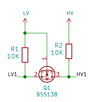
Note: Im basing this on how I believe this level shifter works.
(I could have this wrong)
When both LV1 and HV1 are are neither supplying power nor draining power, LV1 will be LV via R1 and HV1 will be HV via R2.
When HV1 is pulled down, LV1 is also pulled down via the Diode in Q1, i.e. 2-3
When LV1 is pulled down, then it opens 3-2 and also pulls down HV1
That is about it for the simple bi directional converters. I think there are more complex ones involving OPamps and capable of a bit of line driving but I reckon most of the ones referred to would be the cheap?? simpler types as you described with possibly some minor differences.
I have not had anything much to do with these as I try to stick to 5V. This seems to be somewhat more forgiving than 3.3V devices. It is my personal belief that for a beginner at hobby level mucking around with the less forgiving 3.3V or especially a mixture is a mistake. There are too many paths for errors and the beginner, if starting too far up the tree, will end up going in circles not quite knowing where he (or she) has finished up or what happened to “fix???” it.
I think this is evident in many posts on this forum and any with that I can help with I try to encourage the research on some basics as I think this makes further learning much easier. Even the humble ohm’s law familiarity will make life easier.
Cheers Bob
Even on this thread there seem to have evolved pull ups on pull ups on pull ups so no one really knows where everything is at the moment. I think it is time to do as suggested above and get something on paper to sit down and try to work out just what is really happening.
And what about all the others, either added or existing on the sensors ???
That makes some sense. The clock signal seems to go low about one half the clock period after the first negative data transition.
What I don’t understand is there is absolutely NO coherence after that. And another clock excursion low at the end which bears little resemblance to the rest of the clock timing.
This is almost as if the A and B (clock and data) trace have separate time bases which I don’t believe. I have been under the impression for a lot of years that everything revolved around the clock timing. In this case nothing seems to be coherent at all.
I think I have UNO talking with I2C to a 1602 display so when I get a moment I will have a look at that to see what goes on.
Cheers Bob