I2C design constraints

Yeah if you get a good data sheet it will show all the timings.
there are a few things going on that all can be a bit different.

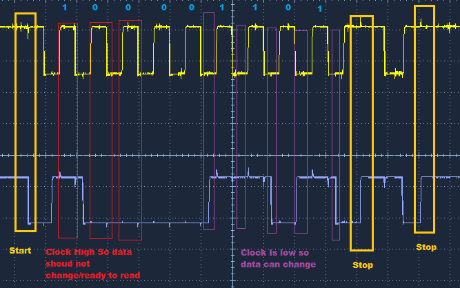
  1. There will be a start condition (is different)
    This will be the data line getting pulled low, while the clock is in a high state.

2.There is the data bits from the master to the slave (master clock)
Data state can change while the clock is low, and is read when the clock is high.

  1. the data from the slave back to the master (master clock)
    Data state can change while the clock is low, and is read when the clock is high.

  2. The stop condition (which will look different)
    the data line will go from low to high while the clock is High.

Note how the start and strop “condition” is inverse from the data change

Something like this mark up, not this is for example only so I may have missed one or two things.

But not 100% sure what is happening at the end
9 bits seems about right. 7 Bit address, 1 R/W bit 1 Ack/Nak bit

for reference, this is not too bad
https://www.analog.com/en/resources/technical-articles/i2c-primer-what-is-i2c-part-1.html

Hi Michael
Thanks heaps for that. I will have a look at the link a bit later.

That all makes sense and looks a lot clearer (to me anyway) now.
Unfortunately during my working life I never did have to go into these finer details. All these bits had all been sorted and designed before my sticky little fingers had a go. Either worked or it didn’t, mostly worked.
In reality I had enough analog problems and what goes with it to get too far down into this digital stuff so I mostly did not have the time to get too involved. I suppose you could say I just knew enough to be dangerous. Unfortunate in one respect I suppose but I figured this digital information had to become analog somewhere otherwise what can you do with it if it has to be used some distance away. The transport mechanism (RF) is analog. Even the modem I am using to send this.

Anyway, thanks again. I will get there or at least a bit further.
Cheers Bob

@Gerard163258 Any chance for a copy of the full source code (I understand if you prefer not to)

Im not sure about the scope screen shot i marked up.
I can see the start, then
1000011 0x43 (which may or may not be a valid address for the devices you have)
0 Read/Not write
1 NAK - So no slaved answered to that address.

While all that can be normal, i.e. your doing a scan; that device was not connected etc.

Next We can see the stop condition… so all that seems ok

But then we seem to have a SDC change while the clock is low but outside a frame, then a 2nd stop condition.

So I am wondering if there is a code bug somewhere. i.e. a clock tick after the first stop then a 2nd stop.

Yes, it’s just test code derived from Arduino IDE test snippets but it works OK on the ESP32 with the JTAG interface.

I’ll dig it out.

// --------------------------------------

// i2c_scanner

//

// Version 1

// This program (or code that looks like it)

// can be found in many places.

// For example on the Arduino.cc forum.

// The original author is not know.

// Version 2, Juni 2012, Using Arduino 1.0.1

// Adapted to be as simple as possible by Arduino.cc user Krodal

// Version 3, Feb 26 2013

// V3 by louarnold

// Version 4, March 3, 2013, Using Arduino 1.0.3

// by Arduino.cc user Krodal.

// Changes by louarnold removed.

// Scanning addresses changed from 0…127 to 1…119,

// according to the i2c scanner by Nick Gammon

// Gammon Forum : Electronics : Microprocessors : I2C - Two-Wire Peripheral Interface - for Arduino

// Version 5, March 28, 2013

// As version 4, but address scans now to 127.

// A sensor seems to use address 120.

// Version 6, November 27, 2015.

// Added waiting for the Leonardo serial communication.

//

//

// This sketch tests the standard 7-bit addresses

// Devices with higher bit address might not be seen properly.

//

#include <Wire.h>

// Pin definitions

const int Blue = 23;

const int Green = 27;

const int Yellow=32;

const int Red=33;

void setup()

{

Wire.begin();

Wire.setTimeout(100);

Wire.setClock(16000);

// Initialize pins as outputs

pinMode(Blue, OUTPUT);

pinMode(Green, OUTPUT);

pinMode(Yellow, OUTPUT);

pinMode(Red,OUTPUT);

// Set initial state to LOW

digitalWrite(Blue, LOW);

digitalWrite(Green, LOW);

digitalWrite(Yellow,LOW);

digitalWrite(Red,LOW);

Serial.begin(9600);

while (!Serial); // Leonardo: wait for serial monitor

Serial.println(“\nI2C Scanner”);

}

void loop()

{

byte error, address;

int nDevices;

Serial.println(“Scanning…”);

nDevices = 0;

for(address = 1; address < 127; address++ )

{

// The i2c_scanner uses the return value of

// the Write.endTransmisstion to see if

// a device did acknowledge to the address.


Wire.beginTransmission(address);

delay(5);

error = Wire.endTransmission();

delay(5);


if (error == 0)

{

  Serial.print("I2C device found at address 0x");

  if (address<16) 

    Serial.print("0");

    Serial.print(address,HEX);

    Serial.println("  !");

    digitalWrite(Green, HIGH);

    nDevices++;

}

else if (error==4) 

{

  Serial.print("Unknown error at address 0x");

  if (address<16) 

    Serial.print("0");

    Serial.println(address,HEX);

    digitalWrite(Red,HIGH);

}    

}

if (nDevices == 0)

Serial.println("No I2C devices found\\n");

else

Serial.println("done\\n");

Serial.printf("Current I2C clock: %lu Hz\\n", Wire.getClock());

delay(500);           // wait 0.5 seconds for next scan

digitalWrite(Red,LOW);

digitalWrite(Green,LOW);

}

thanks, it seems OK from what I could see.

Any chance of the PCB cad files ? Im happy to exchange in private if needed.

I just want to see if anything jumps out, and a bit hard to trace when changing layers :slight_smile:

Note: Im also happy to do an 1 on 1 Video chat where we can run some tests and confirm things (just need to agree on a time as I work normal hours here (so need to be outside the 8:30am - 5pm range.

1 Like

Late joining this thread… some interesting challenges!

I saw this some months ago… our friends at Element14 did some envelope-pushing tests - without any boosters, and got I2C running happily over several meters… using coax. RG58, I think. Check it out here

Clearly, sorting out what is causing the glitches on the SDA line on the DSO is crucial, but coax may be worth considering if twisted pair doesn’t cut it.

Cheers,

T.

2 Likes

Hello All,

I found out that ChatGPT can take a KiCAD schematic and analyse it for feedback.

This is some of it’s thoughts on the I2C issue (which I have had to leave for a bit).

Edit: Chat can also examine PCB files, either Gerber of just a PDF

Hi Michael
Firstly thank you again for that link explaining a bit about the I2C system. Along with the bit I found below on the Df Robot wiki under the link “LCD1602 Datasheet” below.

Which shows the format required by the 1602 display offered by Df Robot and Waveshare, they appear to be the same thing. When I purchased this as a Waveshare device I found the Library supplied or linked absolutely useless. It would only accept text enclosed in “ “ and anything resembling a number reproduced unrecognisable gibberish. Tried just about everything I could think of but the only thing I got on the top line was “Waveshare” and rubbish on row 1 Gave up until someone a while ago suggested a Df Robot library. This worked so I have been experimenting with it a bit. I did not associate Waveshare and Df Robot until the other day when I spotted a label on the back which read “BLWBBA” which I googled. It turned out both companies share the same device. The difference being the Df Robot library works.

My experiment:

Freetronics Eleven (UNO R3) connected from default I2C pins as per wiring diagram in instructions to LCD1602 display (Waveshare) via Gravity connector and open wires 300mm long.

Sketch displaying “Waveshare” on Row 0 which is done in the set up phase. The loop phase reads the elapsed time and displays this on Row 1 in seconds, refreshed at 1 sec intervals. Pretty simple test.

The following is a series of oscilloscope screens

Oscilloscope FRNISI tablet. Has some shortcomings but purchased for convenience and portability. Also is extremely easy to capture and recover instrument screens for publications such as this.

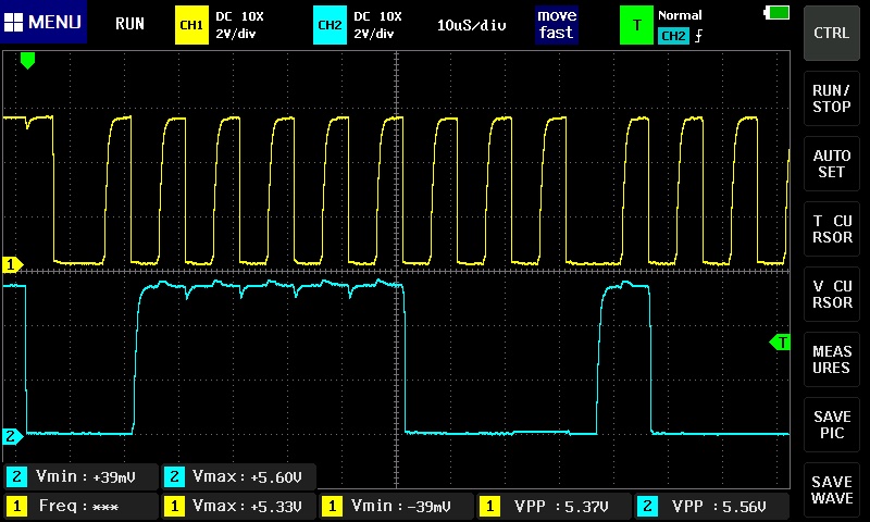
No 1 is the same as the subject of this thread. The address Byte at the same settings as under discussion. Except mine is 5V.


This clearly shows the Start bit, address bits (0x3e), R/W bit (W) and ACK/NACK bit (ACK). The next pulse turns out to be the start of a “control” Byte.

No 2 is a pic showing most of the 3 Bytes in this group

The first Byte is as above, the second Byte is a “Control” Byte, the third is probably the start of info possibly cursor position (0,1 column 0 row 1). Not exactly sure about this.


The second Byte clearly shows the Control byte as 10000000 plus ACK bit as 0.

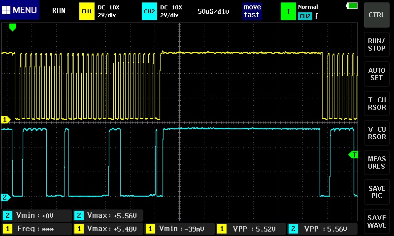
No 3 is a pic showing the first 3 bytes and the start of the second group


The third Byte looks like 11000000 plus ACK bit as 0 followed by an unexplained pulse and a stop bit. The start of the next group appears with looks like the start of another address Byte

one of the shortcomings of this osc is the lack of a delayed sweep function (I can’t find it anyway) so am unable to expand the end of the 3rd Byte to look at timing of this strange pulse. Trouble is that I2C is a 2 way street so is a bit difficult establishing where this pulse originates.

Anyway I fired up my old ATTEN scope which has some faults (failed XY and suspect attenuators) but the delayed sweep does still work.

The result below


This “phantom” pulse is shown immediately following the ACK bit and followed by the Stop bit. Mystery, to me anyway. But there are still lots of things still a mystery to me so it might turn out not so strange after all.

Sorry to be a bit long winded but I said I would do this so here it is.
Cheers Bob

2 Likes

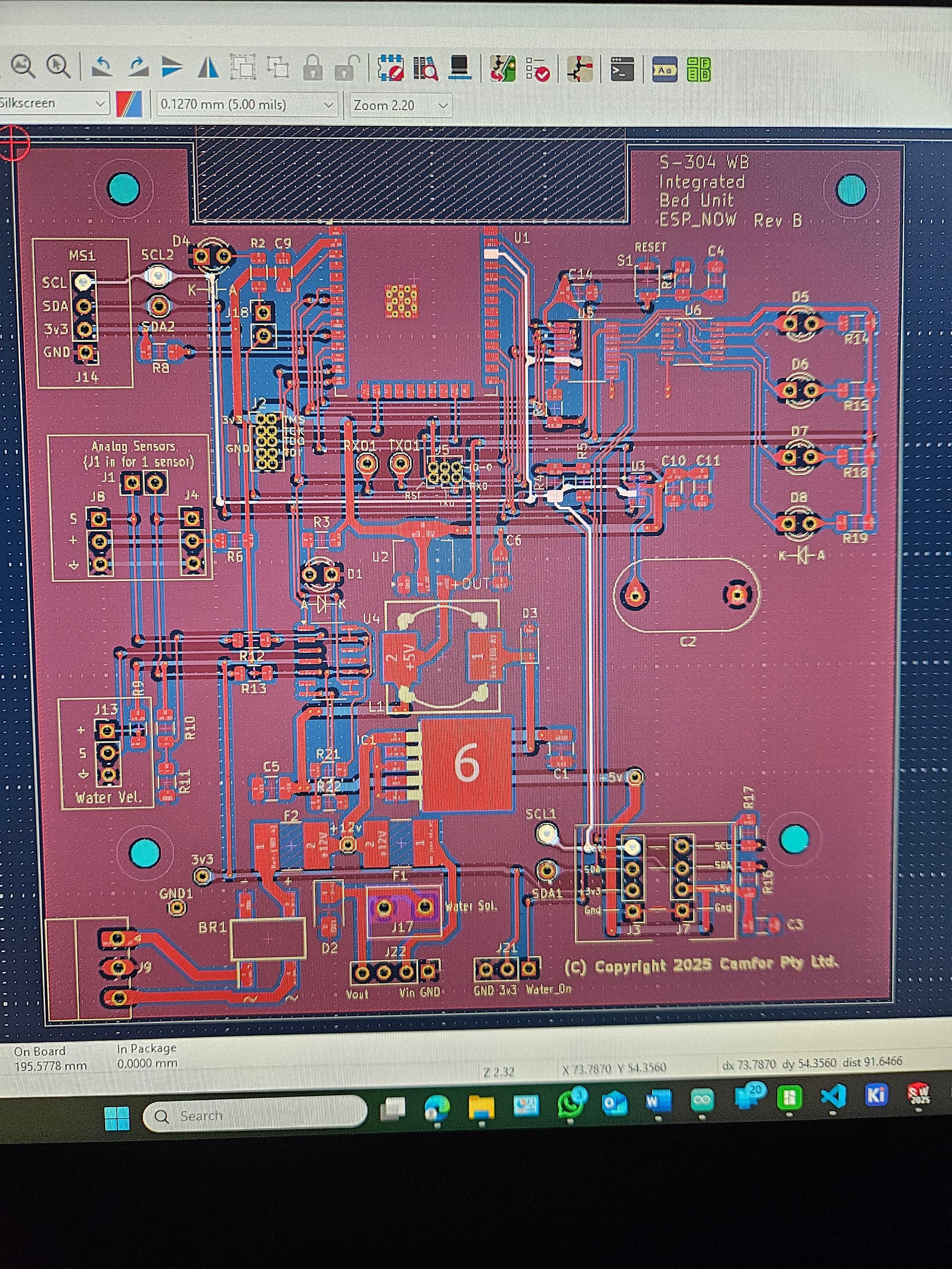
I had a look at the PCB traces…..

SCL is highlighted and SDA is very similar in trace layout.

The trace looks OK and it’s similar to other I2C layouts I’ve done. Having said that, I think the I2C connections at the bottom of the PCB can go. They were really a remnant of the previous, more complex iteration. Also, can probably get rid of the level shifter. It was necessary back when we had an RS485 implementation but we use ESP_Now for the comms. You can see the small tail going to U3 which is the RTC.

1 Like

Turns out I’ve been doing a lot of the same thing the last several days… examining and trying to decode I2C traces on my scope, as I prepare my own PCB with a couple of I2C ports.

I have two things that others might find useful:

  1. I put together a system to capture one-off shots on my scope, using a GPIO pin to activate the EXT trigger on my scope (assuming you have one…mine is a Hantek DSO5102B), with SCL and SDA on the two main channels
    This, coupled with a bit of code I wrote allows me to quickly generate traces of various things, eg writing to an LCD1602, or reading a TOF distance sensor… or doing things with an OLED. Saves me a bit of time…see attached.
  2. For those of us too poor to afford a decent logic analyser… I found this a while back. Now costs about $8… but seems to do a pretty decent job decoding I2C protocol…Cheap Logic Analyser
    I will order one real soon, and can report if it lives up to the claims.

ext_trigger.zip (948 Bytes)

Cheers,

T

2 Likes

@Gerard163258 Im knida just wanting to be able to trace what goes where to see if anything jumps out.

While a scope is good at checking out the actual signal, so things like noise shows up. A logic analyzer (even a cheap one) can go a long way to seeing what happens. A lot of the time we can see a non-perfect wave (e.g. may have a very small spike and/or a ring etc) but this may or may not be an issue for the actual comms.
A lot of digital systems tend to have one voltage that needs to be passed for a 0 level detection and a separate voltage that would trigger a high logic level. such that anything thats between those 2 levels is a kinda no-mans-land. This helps with low levels of ripple noise.
e.g.
ESP32 3.3V
Low Level : anything less then : 0.825V
High Level : anything higher then : 2.475V

@Robert93820
I see I2C and other comms protocols as just the protocol to exchange bits between the end points.
The actual data structure like command/control/register etc is more just what is needed for a specific device.
so I2C would be <R|W><8 bits of data>…<8 bits of data>
Some systems are 1 byte exchange. e.g. read from memory/register location XX.
On thinks like displays, the big challenge is there are lots of driver chips and some cheap vendors may not label this correctly.
e.g. SSD1306, SH1106 are very close to each other with all the same commands and screen sizes. But the SH1106 cols 0 and 1 are off the screen so needs tweaking to “shift” your display over by 2 columns. If not you can get what looks like mostly random dots as everything gets mis-aligned.

But I feel I am not drifting away from the OP challenge; so I will pull back to that. (More then happy to keep discussion going in a new thread)

1 Like

One thing I keep thinking of is cross talk between tracks. some of the lines are thin and close.
On analysis of one of your scope images it very much looks like the change of “level” of one line had an effect on the other. This could be due to cross talk; if this is an issue then its a PCB layer fix.
That said, im not sure that amount or “signal noise” would really affect the actual I2C comms. i.e. IF you were going to make a new version of the board, then ensuring a ground plane under the comms traces and maybe a bit more space between the tracks. (i.e. if you have the space).

Im getting a little bit lost now as to what is the capture of a failed coms is in your setup.
i.e. if you have things that are working, great. Do they have some noise and working, this could be OK. So what I think I need is a fresh copy of a scope capture where the I2C is failing. In this capture we need to ensure we can see each clock pulse clearly so we can if it shows something really bad.

1 Like

@Michael99645 I am deeply envious of your nice square clock pulses! Mine (and Bob’s) look much more rounded. At 400kHz, a blown-up transaction looks like this on my prototype (ie breadboard, 20cm plain wires from a Core Splitter:to my DSO probes… not ideal, I know…), using a Hantek DSO5102B (and yeah I forgot to set the date ;-( )

They look much nicer/squarer at 100kHz… but yours are awesome! What frequency, pull-ups etc and physical setup created the trace in your post #41 ??

Regards, T.

1 Like

In my example it was an ESP32-S3 talking to an OLED display. some connection wires connecters direct between the two. I used the IDF for ESP32 c code, and not arduino libraries, so when I set up the I2C i told it to add the internal pull ups. While this is fine for my 1:1 use it may or may not be the best way for your setup.

Looking at your latest scope image, the pull down seems fast, but the rise time is slow. To me that says either
a) the pull ups are too weak, thus taking longer to “charge” the bus.
b) there is some “pull down”/leak that your pull ups are fighting against.
c) there is some resistance on the bus (between your pull up and probe point)

One thing that kinda seems weird to me is with a div of 2v the looks to be about 4V; which is neither 3.3v or 5v

1 Like

Yes, that’s what I was thinking too (crosstalk). I’ll see if I can get some shots of the I2C when it’s broken. The SDA runs adjacent to SCL everywhere on the PCB.

Hi Michael

I make the yellow trace about “3 and a bit V” and the blue trace similar.

Trevor: if you align the ground market with a screen graticule division it would be easier to interpret.

Item a. I would agree with that. With my Waveshare display (unpowered) I measure 20k between SCL and SDA which would suggest 10k pull ups on each to “somewhere” This “somewhere” is not VCC as from each to VCC I measure about 500k rising (cap charging???).
I don’t know what is going on as the Waveshare Wiki says pull ups ARE fitted but in the absence of a schematic I don’t know just how this is done. But it seems to work. I will try later with a device that has physical resistors that I can see.

Item b. If this were so you would effectively have a voltage divider. trevor does not state a VCC but I assume it is 3.3V and if there was a pull DOWN I think the pulse would be much lower.

Item c. I think there would have to be a bit more than track and wire resistance. If using the probe at 10:1 (if not you should be) the input resistance will be 10MΩ so any stray at this point should not even affect the probe response. If it did, the rounding would appear at the negative going transition also.
Cheers Bob

1 Like

Thanks gents. More testing required!

Yes I adjusted vertical position after I took those traces… next time will be aligned to a major graticle.

I am using Core’s Pico Dev platform, it provides a nice Qwiic connector… and has built-in 4K7 pullups, confirmed on both circuit schematic and with VM.

Recently I looked my Waveshare1602 under the microscope… I could see 6 (yes, 6) 2K2’s placed right near the I2C pins. Could not precisely trace all of them, but certainly looks like both SDA and SCL go via at least one each.

My scope traces were taken from a Core I2C splitter… the scope probe ground is connected to the I2C GND, and measuring SCL & SDA, all coming out of the splitter. I too was puzzled by the amplitude.. I’ll do another test and have the scope measure it…

I’ll update this post with pics ASAP…

1 Like

Hi Trevor

Same as mine.
There are also 2 x 10k resistors near the VCC end of the connector. These connect directly to SCL and SDA (1 to each). The other end of the resistors connect together but I don’t know to where. Certainly NOT to VCC. They seem to be the pull ups but it would be nice to know pull up to WHAT. A schematic would be handy but seems not easily forthcoming.

I might add this is the only Waveshare bit I have and probably will be the only one unless there is a bit more info available. My personal opinion.
Cheers Bob

1 Like

I found this pdf that might help track down whats going on.

2 Likes