Hey everyone
Thank-you everyone for your thoughts so far. 
I’m glad to provide you all with a good mystery. 
Let me reply to everything below.
Do you mean the reset pin? 
Yeah they’re operated to the PG pin of this 5v voltage regulator via a FET. On boot, the power good (PG) pin of this regulator is low for a fraction of a second until the VCC output is stable.
Once the regulator has settled then PG goes HIGH and that’s where it stays.
The 555’s and 74hc73’s reset are both active low. All reset pins are tied together with the PG reset vector from the regulator. I should have shown this in the video to remove ambiguity. My bad.
[quote=“Michael99645, post:5, topic:22503”]
Is the clock signal at the JK as ot seems to be inverted from the 555 ?
[/quote
Yes the debounced button is inverted. The inverted debounced button goes to pin 1 which is the clk of the negatively edged triggered 74hc73.  J&K are both tied high. This is to get me that toggle effect. I’m basically turning my momentary button into a switch with a long cool down.
That’s actually a really good thought.
I’m not really using this HC chip as it was intended. It’s probably expecting a 250mhz clock and a register that samples the signal in a certain period of time.
Great question.
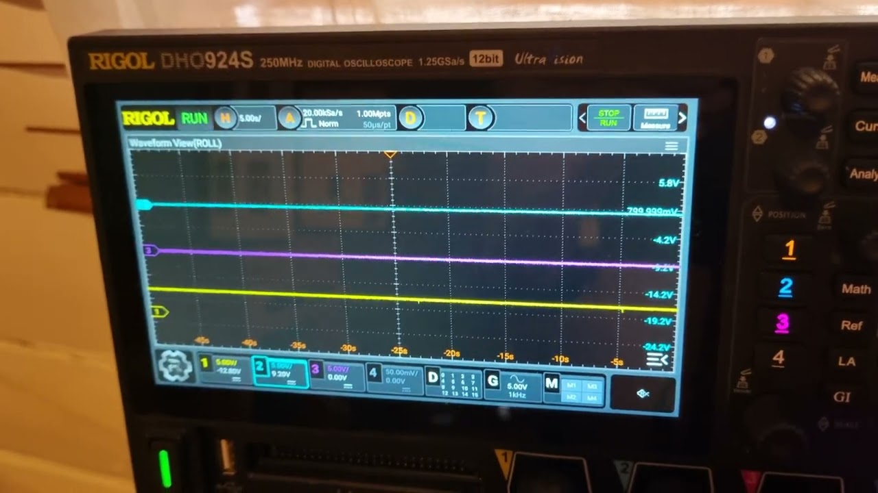
After. The Oscilloscopes yellow is the collector of the transistor (Q1).
Good thought. There was no relay plugged in during those oscilloscope measurements so we can rule that out. 
In order to stay alive I have developed a low confidence in all of my designs… so no not really 
Ah bummer. I rushed the schematic and I got it wrong. Let me clean that up.
At the last second I’ve added the 100nf capacitor that was on the rails of my bread board but In doing so I’ve disconnected the button from ground and gave it a pointless 5v. 
The good news is that, although the schematic was wrong, my circuit was correct. 
The schematic below is now reflective of the actual circuit I’ve made.
Here is another version with an added cap to pin 4.
I’ve re-annotated the schematic.
R2 & C1’s time constant should now be a little over a third of R3 & C3’s.
I’m not sure this RC filter will work because the reset vector itself is essentially tied high.
Maybe I need to consider removing the reset vector entirely.
More on the RST/CLR signal
OK I want to provide as much detail as possible on the reset vector since it’s the most likely culprit.
Through testing, I learned that the PG output has very little current capacity. It won’t even drive a little led. I added a 2n7000 n channel mosfet just to ensure a nice clean 5v reset.
The reset signal is going to go to many different chips and modules in my project. Each module was going to have there own ~1k ohm pull down resistor.
Maybe I should consider putting a pull down resistor at the source of the mosfet instead. 
Here is a super quick and dirty schematic.
Happy to measure the quality of that reset vector if we think it has merit.  .
.
![]()


