Need guidance in photodetection part of DAQ system

Hi,

I am currently working on a project to develop a fibre optic dosimetry system. The system uses an organic scintillator (BCF-60), which emits green light at 530 nm and has an active volume of 0.8 mm³.

As part of the project, I am designing a transimpedance amplifier (TIA) circuit using the S1223-01 photodetector, which I selected based on its spectral response range (360 nm to 900 nm) and photosensitivity (0.1–0.6 A/W).

To simulate a clinical environment, I use a function generator to produce a 360 Hz pulse signal, which drives a 5 mm green LED. The light signal is transmitted through a 2-meter-long, 1 mm diameter fibre optic cable. The other end of the fibre is coupled to the photodiode, which is connected to the TIA circuit built around the OP07CP op-amp, using a feedback resistor of 1.1 MΩ. The output of the TIA is then connected to a second-stage amplifier (a voltage follower using the OP276) configured with unity gain.

However, I am currently experiencing noise in the output signal, and I plan to test the setup using a National Instruments DAQ (NI 6363) for further analysis.

I attached circuit diagram in which I am using TIA (OP07CP) I am getting noise of around 100 mV at output of TIA. kindly please guide me how I could reduce this noise.

1 Like

Hey @Hasham276047,

Sounds like a really interesting project! A few ideas you might try:

  • Experiment with different values for Cf for example, 33 pF and 100 pF. Your current 10 pF sets a single-pole corner around ~14.5 kHz, which is well above your 360 Hz signal. That can let amplifier noise, oscillation harmonics, and EMI sneak in.
  • Add 0.1 µF ceramic and 10 µF electrolytic capacitors at the op-amp power rails, positioned as close to the pins as possible.
  • If you’re not committed to the OP07CP, consider something like the OPA657 .
  • Try placing a small series resistor at the diode (between 10–100 Ω) to see if it helps with stability or noise.

Otherwise, @Robert93820 may have some great ideas :slight_smile:

1 Like

Hi Hasham
That is a strange circuit. I would have to do a refresher bit of research to figure out exactly what is supposed to happen. I can’t see anything much happening actually.
The photo diode has no return path via ground. Once the C (C something, I wish people would assign component numbers to make it easier in describing things) has charged it will just sit there doing nothing as there is no discharge path that I can see .

I don’t know how the first OpAmp works. Signal (???) applied to non inverting input. Inverting input ground. Feedback (positive) from output to + input. OpAmp is going to try and do whatever it takes to keep both inputs the same (Ground) so what will appear at the output would be anybody’s guess at the moment anyway. Might actually be an oscillator.

Noise comes in various forms. Could yours be the resiult of the first OpAmp oscillating ??
An Oscilloscope picture would be a help here.

The second OpAmp is simply a voltage follower presumably to provide some form of isolation and a low impedance source for the final OpAmp.
Which is an inverting comparator with some hysteresis provided by the positive feedback resistor. There should be a resistor between the reference voltage and + input which I think makes the hysteresis more predictable.
By the way you have not shown what you do with the LM311 emitter output (Pin 1) Should be grounded in this case.

Just at the moment I have no idea what the N!6363 does.
Cheers Bob

3 Likes

Hi Hasham
I just had a quick Google of “transimpedance amplifier”.
Wikipedia have an article on the subject.
Looking at that article you would appear to have your OpAmp inputs reversed. You could try connecting Cathode of Photo Diode to - input and ground to + input. I think the Photo Diode anode should be ground. Remove that capacitor.

This could also be a mistake with your circuit drawing. The + and - inputs could be shown reversed.
Cheers Bob
Edit
“OpAmp” should read “TIA OpAmp”.

2 Likes

Hi,

Sorry for late reply, I updated the circuit diagram and it is attached. I’ve been testing it using a 360 Hz pulse signal. When varying the duty cycle from 50% down to 0.8%, the system performs smoothly. However, when I reduce the duty cycle further to 0.3% or 0.2%, I start observing significant noise, both on the oscilloscope (wave signal of TIA and comparator output) and in the data captured by the DAQ, which is no longer registering correct values.

I also tried changing the TIA’s feedback resistor (Rf) from 1 MΩ to 2.2 MΩ, but the issue persists.

How can I reduce or eliminate this noise so the circuit can operate reliably at a 0.2% duty cycle?

Kind regards

Hasham

1 Like

Hi Hasham
Which trace is Ch 1 and Ch 2. I am guessing the square is Ch 2 comparator output at 5V and the other is Ch 1 at 736mV.
Exactly where are you measuring these waveforms.

I note you have reversed the inputs to TIA and removed the series diode cap. That bit seems to work.

I also note the OP276 is now an inverting unity gain amplifier. This was previously a non inverting voltage follower. What happened here. Did you find this output the wrong polarity?

Looking now at the output at the lower duty cycle. It looks like your “noise” could be the comparator not being able to make up its mind whether to switch or not ; not much hysteresis.
The reference voltage calculates to 0.318V which is about what it is switching at (2nd pic) but the “noise” looks like switching action due to lack of hysteresis. It is trying to switch at nearly the flat top of the input. More level here I think would help. You could try increasing the gain of the OP276 by increasing the feedback to 15k or 20k.
For “proper” operation of hysteresis there should be a resistor from the reference voltage at the junction of R1 and R2 (very hard to read detail.Get the camera square on with the paper so it focuses the same all over or scan the sheet) and the comparator + input. Hysteresis is dependant on the ratio between this resistor and the feedback resistor which I think could be R4 (1Meg).

There are hysteresis calculators on line. Here is one
https://www.allaboutcircuits.com/tools/hysteresis-comparator-calculator/
Cheers Bob

1 Like

Hi,

Thank you for your response and for sharing the comparator calculator — it was very helpful.

I would appreciate your guidance on how to select the optimal values for Rf and Cf in my TIA circuit, to ensure a clean and sharp pulse signal. I am currently using the S1223-01 photodiode and have replaced the TIA op-amp from OP07C to OP276.

Additionally, when I connect the trigger input of my DAQ system to the comparator’s output, I observe a voltage jump on the comparator output signal (as seen on the oscilloscope). Could you kindly advise on what might be causing this and how I can resolve it?

Looking forward to your suggestions.

Kind regards,
Hasham

1 Like

Hi Hasham,

It might be worth keeping all of your posts in the one topic so new members can scroll through and get context.

Could you please send through a photo of your physical circuit?

Quickly confirming Bob’s question will help immensely.

Liam

Hi Hasham

You are not going to get much if you don’t do as asked and answer some questions.

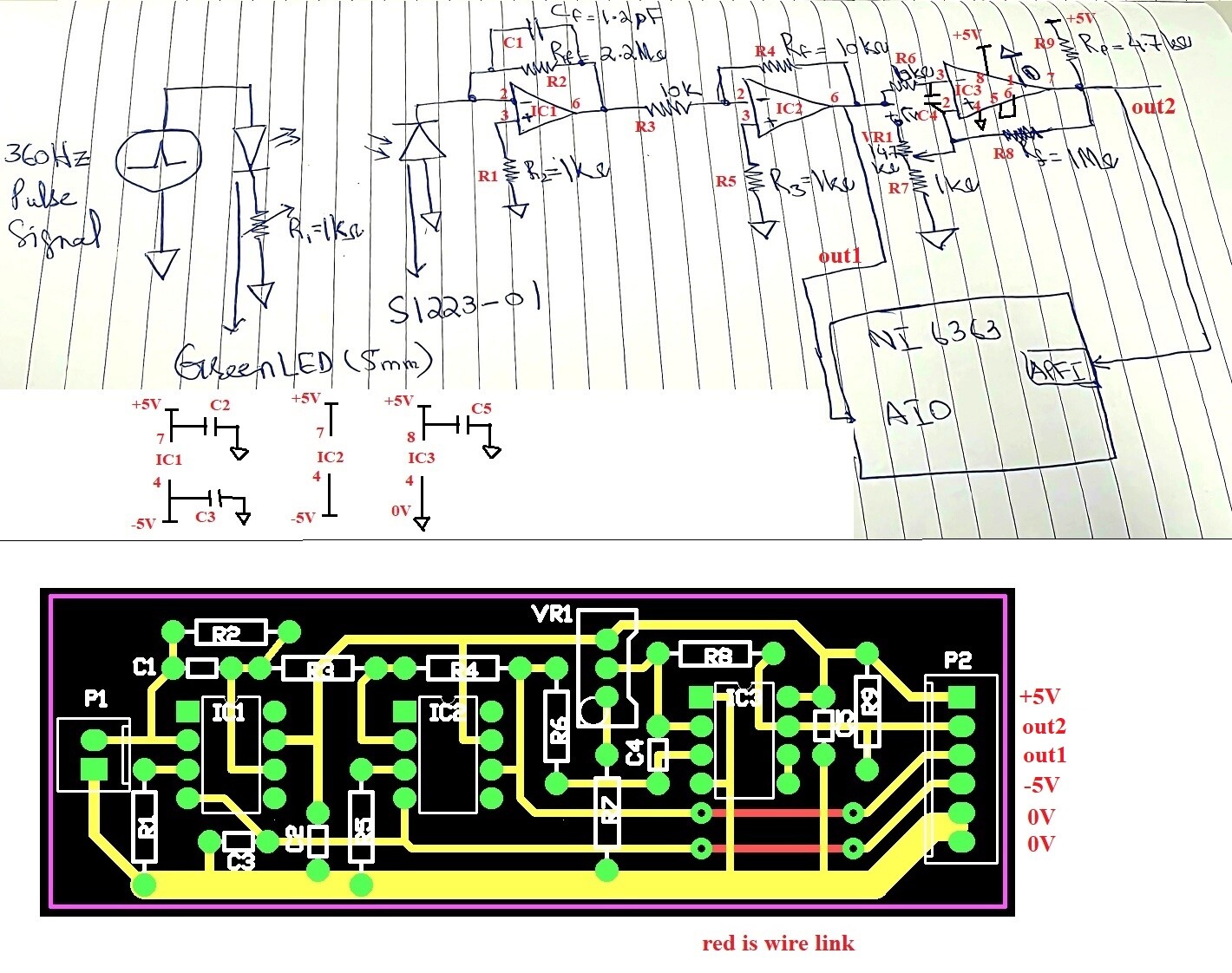
You have NOT annotated the schematic components to make answering easier as I asked you do.

You have NOT said where EXACTLY those scope pics are measured.

Were those measurements taken before or after the TIA feedback (would be much easier if I could quote R?? instead of a description) resistor was increased from 1.1MΩ to 2.2MΩ.

Could you separate the scope traces so we can see exactly which one has this “nose” on it. Can’t tell when the traces are superimposed.

General: I am assuming the power supply is still +5V/ -5V you have referred to as “Bias Supply”
I think your 0.2% duty cycle could be a bit ambitious. At this figure the pulse width should be 5.56µSec. Looking at your pic it is taking about 7 or 8µSec to reach the comparator switching point. This pulse has a finite attack time and a relatively long decay time. Probably due to the Rf/Cf time constant.
I still think your "noise " looks like comparator switching instability due to not enough amplitude of the input signal and the fact it is trying to switch as the input signal reaches its peak. And the omission of the 10k resistor I suggested between the reference point and + comparator input. I don’t think any hysteresis will work properly without it.

You seem to have built up a complete system and then trying to trouble shoot. This is really not the way to go about it.

Suggestions
Disconnect the NI 6363. Do this at the op amps, don’t leave any little antennas floating around.
Disconnect the inverting amp (call this Q2)
Connect a temporary 10kΩ between Q1 output and ground.
Apply nearly 100% duty cycle to transmitting LED (call this D1).
Measure the current of photo diode (call this D2). You should be able to do this fairly accurately by measuring the voltage between Q1 output and ground and dividing by the feedback resistor. Volts divided by R in MΩ will be µA. Alternatively measure the V across Rf and do the same. In this case the 10MΩ resistance of the DMM will have to be considered. This will be in parallel with Rf. The result should be very near the same.
Is this what you expect. If not find out why. Looking at your scope pix I think this will be in the order of 0.68µA if Rf is 1.1MΩ and 0.34µA if Rf is 2.2MΩ. I am guessing here using the pulse peak at the inverter output of about 740mV as a basis. Should be close as the inverting amp is unity gain at this stage if one can believe the schematic.

Note “0.34µA” was 1.68µA. See edit below.

Apply your signal at say 20% duty and have a look at the waveform. Expand so you can see the attack and decay slope. Check at 0.2%. There are a few contributing factors here. D1 response time, D2 response tome and the R/C time constant in the feedback network. Try removing Cf. What slope remains will be the diode and possibly the OpAmp responses, there is not much you can do about that except maybe find a better TX diode. D2 is a dedicated photo diode bur should be OK. Worth checking data sheet though. You might need some experimenting with feedback components here.

When you are satisfied this stage is OK you can then go on with the next.
Disconnect the comparator and do the same, connect a temporary 10k from Inverter (call this Q2) to ground. Adjust the gain (by changing the feedback R value) for a suitable level at the output to operate the comparator reliably. If you get a decent level you won’t need much hysteresis but you should have some to get good switching without any “chatter”

You can reconnect the comparator. You will need the resistor from reference V to + input (suggest 10kΩ) for any hysteresis calculator to work (I pointed this out above and according to your updated schematic this has been ignored), as I said previously it is the ratio between this resistor and the positive feedback resistor (I think R4 in your schematic, out of focus so difficult to read properly).
Check the output for a good clean signal.

You could well be putting it there with your scope probe earth lead. This should be as short as practical and connected to a ground as close as possible to the measuring point.

Once you are satisfied and only then re connect the NI6363 and do whatever you do with it. If this spike mentioned above re appears only when this device is connected this will be something else again which I know nothing about. It may be possible to ignore it anyway.

One very important thing here. The above description has dismantled the system and got (hopefully) one stage at a time working. Finishing up with a whole that should work OK.
If you make changes do so one change at a time. And record results somewhere. You seem to have made several changes at once here, The photo diode input, the feedback resistor (Rf) value, The buffer from non inverting to inverting and apparently op amp type. This is an absolute no no. You will keep going in circles if you do this sort of thing. You also published scope screen shots ad did not specify at what stage these measurements were made It does help immensely if you can be more specific and please be as accurate as you can. Saves a lot of time and effort when helping.
Cheers Bob

EDITED: "1.68µA above changed to 0.34µA 1005AM 30/09/25

2 Likes

Sorry for the late reply, I am using an oscilloscope and DAQ NI-6363 to capture points..

1 Like

Thanks for that @Hasham276047

Could you you please send through a photo of your circuit? It will be a lot easier to diagnose problems if we can see it.

And did you get any results from following Bob’s suggestion?

1 Like

Hi Hasham
Doesn’t really answer ANY of the question.
I asked you to define EXACTLY where these scope probes were connected, which I can probably guess, and under what exact circuit conditions. This is important as you have changes the circuit and component values.
Cheers Bob
PS I KNOW you are using an oscilloscope, funny enough you can tell by the pictures. I have no idea exactly what the NI6363 does but I do know you have no use for it until you get something to look at. Get that bit right first.

Hi,

I sincerely apologize for the delayed response, and I’m very thankful for your suggestions. Following your advice, I corrected my circuit and transferred it to a PCB board.

Last week, I performed my first photodetection test using a real radioactive source — the Ir-192 HDR source — and I was successful in detecting the signal.

During the hospital visit, I initially encountered significant noise. I first changed R2 from 2.2 MΩ to 100 MΩ, but the noise persisted. Then, I disconnected pin 2 of the TIA op-amp (IC) from the PCB and connected it directly to the photodiode and R2, which helped reduce the noise slightly, but I still didn’t get a usable signal.

Finally, when I changed R2 to 1 GΩ, I was able to successfully detect the photodetection signal. I also cross-checked the performance using a commercial Gigahertz TIA amplifier, and the signal level from my circuit was of the same order of magnitude — approximately 10⁹ V/A.

Last week, I also tested my circuit on a LINAC by irradiating it with a 6 MeV photon beam. However, in that case, I failed to obtain a pulse signal — I only observed noise.

Could you kindly guide me on how to obtain a clear pulse signal from the LINAC? I’m considering increasing the R2 value from 1 GΩ to 10 GΩ, but I understand that this may reduce the bandwidth of the TIA.

For reference, I am using the CA3140 IC for the TIA stage and the OP27G for the second-stage amplifier.

1 Like

Hi Hasham

You are using this in a hospital??? Possibly for future diagnostic purposes???

Leave me right out of it.

Don’t even know what a LINAC is.
Cheers Bob

1 Like

It’s a medical grade Linear Accelerator. In his first post, Hasham states that he is making fibre-optics dosimetry system.

@Hasham276047, what is your use case for this project would be.

Bob is right, if this is actually being used in a medical use case, this is way beyond the capability of this forum and would require working with a qualified medical equipment engineer.

This is a prototype-based circuit, and I’m doing my best to complete the tasks related to the project. However, I must admit that I don’t have a strong background in electronics, which is why I often post my issues here — and the support has always been very helpful.

At the moment, I’m stuck again. I need to capture the light signal generated by a scintillator when exposed to a 6 MeV photon beam from a LINAC, using my photodetection circuit. Unfortunately, I haven’t been able to detect a reliable signal so far.

Could you please guide me on how I can increase the sensitivity of the transimpedance amplifier (TIA) to better detect this light signal?

I also came across an article discussing T-network-based TIA amplifiers. Would this type of configuration be suitable for my application? Any guidance or suggestions would be greatly appreciated. As already I increased resistance to 1G ohm…KIndly please guide

1 Like

Maybe the photo diode does not respond to the range of frequencies produced by this “new” gadget.
Cheers Bob

2 Likes

However, I’m still uncertain about which op-amp IC is best for achieving very high transimpedance gain, on the order of 10¹¹ to 10¹² V/A. I understand that higher gain can be achieved by increasing the feedback resistance, but I’m unsure how high the resistance can be in practice, and which IC can handle it effectively without introducing noise or instability.

Could you please guide me on:

  1. How to reliably achieve such high TIA gain?

  2. How high the feedback resistor can be in practice?

  3. Which op-amp IC would be most suitable?

Hi Hasham
Have you checked the frequency response as I suggested in my last post.

It seems to me that you want all the information flow to be one way. You never seem to offer answers to any query. Just expect everyone on this side to wave a magic wand.

I think under these circumstances replies are not going to be very frequent.

I will attempt to help with the latest lot of questions

Having nil experience with TIA amplifiers I have no idea.

Open circuit. In this case the OpAmp would probably act as a comparator and become a switch.
I don’t know where you got the 1GΩ resistor from. Not terribly common. Your idea of 10GΩ could be seen as pretty ridiculous even if you could get one. Leakage paths and capacitor leakage equivalent resistance would probably be less than that.

No idea. You will have to start looking or find someone with experience in this sort of thing. Called “Research”
Cheers Bob

1 Like

Dear Bob,

I tested the frequency response of the photodiode by using a green LED as the input source, modulated at 360 Hz with a 1% duty cycle. The photodiode I used (S1223-01) has a spectral response range from 350 nm to 930 nm, and according to its datasheet, the photosensitivity at 550 nm lies in the rising region of its spectral response curve.